In-situ curvature measurements in MBE - Laytec
In-situ curvature measurements in MBE - Laytec
In-situ curvature measurements in MBE - Laytec

Create successful ePaper yourself
Turn your PDF publications into a flip-book with our unique Google optimized e-Paper software.
Application Note 46<br />
<strong>In</strong>-<strong>situ</strong> <strong>curvature</strong> <strong>measurements</strong> <strong>in</strong> <strong>MBE</strong><br />
<strong>In</strong>-<strong>situ</strong> <strong>curvature</strong> <strong>measurements</strong> have become <strong>in</strong>dispensable for monitor<strong>in</strong>g and understand<strong>in</strong>g<br />
the stra<strong>in</strong> relaxation <strong>in</strong> group-III-nitride layers grown by <strong>MBE</strong>. Dr. Yvon Cordier of CRHEA<br />
(France, Valbonne) used LayTec’s <strong>in</strong>-<strong>situ</strong> optical sensor EpiCurve® TT <strong>in</strong> a Riber Compact 21 system<br />
for stress eng<strong>in</strong>eer<strong>in</strong>g to obta<strong>in</strong> thick, high-quality GaN layers without cracks on Si substrates.<br />
The heteroepitaxy of group-III-Nitrides often leads to problems related to stress due to the lattice<br />
mismatch between the substrate and the grow<strong>in</strong>g material as well as the difference <strong>in</strong> thermal expansion<br />
coefficient. The first leads to high densities of thread<strong>in</strong>g dislocations and is associated with<br />
residual stress. The second generates additional stress when cool<strong>in</strong>g down to room temperature. <strong>In</strong><br />
particular, for the <strong>MBE</strong> growth of Ga(Al)N films on SiC or Silicon substrate, the difference <strong>in</strong> thermal<br />
expansion coefficient is responsible for a tensile stress at room temperature, which can generate<br />
cracks <strong>in</strong> the films. Furthermore, the stressed epitaxial layers and the substrate experience a bend<strong>in</strong>g,<br />
which depends on the stress. Excessive bend<strong>in</strong>g and the presence of cracks hamper the development<br />
of devices especially for large substrates where the bow is even more significant.<br />
Stress eng<strong>in</strong>eer<strong>in</strong>g helps to obta<strong>in</strong> thick, high-quality GaN layers without cracks even on Si substrates.<br />
AlN <strong>in</strong>terlayers or AlGaN stress reduc<strong>in</strong>g layers allows the growth of thick GaN films on silicon.<br />
But the efficiency of such procedures depends to a large extent on growth conditions and layer<br />
quality. <strong>In</strong>-<strong>situ</strong> monitor<strong>in</strong>g of stress is therefore a very useful tool for optimiz<strong>in</strong>g such layers.<br />
temperature [°C]<br />
GaN AlN<br />
0.25 µm 0.25 µm<br />
1100<br />
1050<br />
1000<br />
950<br />
900<br />
850<br />
800<br />
750<br />
700<br />
650<br />
GaN<br />
1.7 µm<br />
cool<br />
down<br />
150<br />
temperature<br />
<strong>curvature</strong><br />
100<br />
600<br />
0 5000 10000 15000 20000<br />
time [s]<br />
GaN<br />
1.7 µm<br />
temperature<br />
cool<br />
down<br />
150<br />
<strong>curvature</strong> 100<br />
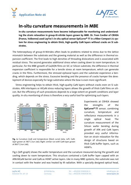
Fig. 1: Curvature (red) and temperature (black curve) data. Left: GaNlayer<br />
grown at 780˚C (run 240). Right: similar run with GaN-layer grown<br />
at 800˚C (run 246).<br />
50<br />
0<br />
-50<br />
-100<br />
-150<br />
-200<br />
-250<br />
<strong>curvature</strong> [km -1 ]<br />
temperature [°C]<br />
1100<br />
1050<br />
1000<br />
950<br />
900<br />
850<br />
800<br />
750<br />
700<br />
650<br />
600<br />
15000 20000<br />
time [s]<br />
Experiments at CRHEA showed<br />
the strengths of the<br />
EpiCurve® TT sensor, comb<strong>in</strong><strong>in</strong>g<br />
<strong>curvature</strong>, temperature and<br />
reflectance <strong>measurements</strong> <strong>in</strong> a<br />
s<strong>in</strong>gle optical head. The<br />
<strong>curvature</strong> measurement of the<br />
Silicon wafer bend<strong>in</strong>g dur<strong>in</strong>g<br />
growth of AlN and GaN layers<br />
provided very useful <strong>in</strong>formation<br />
on stra<strong>in</strong> relaxation for the<br />
design of structures based on<br />
thick GaN buffer layers, such as<br />
HEMTs.<br />
Fig.1 (left graph) shows the wafer temperature and the <strong>curvature</strong> measured dur<strong>in</strong>g the growth and<br />
cool<strong>in</strong>g down to room temperature. This structure conta<strong>in</strong>ed a GaN buffer layer capped with an<br />
AlN/AlGaN barrier and GaN as HEMT active layers. Like <strong>in</strong> many <strong>MBE</strong> systems, the substrate was not<br />
<strong>in</strong> contact with the heater and was heated by IR radiation. With a specially designed optical head,<br />
50<br />
0<br />
-50<br />
-100<br />
-150<br />
-200<br />
-250<br />
<strong>curvature</strong> [km -1 ]
Application Note 46<br />
the wafer temperature was measured very accurately (with an offset due to radiation from the hot<br />
sources of only ≤ 3 K).<br />
Once the growth of the first AlN layer was started, a concave <strong>curvature</strong> was observed. Then the<br />
growth of the GaN layer quickly changed the <strong>curvature</strong> to almost zero. The AlN layer re-established a<br />
<strong>curvature</strong> rise. Although the growth conditions were identical to those of the first 0.25 μm GaN <strong>in</strong>terlayer,<br />
the 1.7 μm thick GaN layer rapidly developed a negative (convex) <strong>curvature</strong> that slowly<br />
saturated after the deposition of about 1.6 μm. The growth of the tensile stra<strong>in</strong>ed AlGaN barrier<br />
layer also contributed to this saturation, before cool<strong>in</strong>g down to room temperature reduced the <strong>curvature</strong><br />
aga<strong>in</strong>.<br />
The development of the <strong>curvature</strong> for the thick GaN layer depends on the growth conditions. Fig.1<br />
(right graph) shows the <strong>curvature</strong> for GaN layer grown at 800˚C (20°C higher substrate temperature<br />
than before). Despite similar RHEED patterns and <strong>in</strong>itial <strong>curvature</strong> quickly develop<strong>in</strong>g towards negative<br />
values, the saturation of <strong>curvature</strong> was faster (after only half of the GaN growth). This is a clear<br />
<strong>in</strong>dication of layer relaxation. This second type of growth structure was not able to compensate the<br />
thermal mismatch. The two times higher density of thread<strong>in</strong>g dislocation on the surface was observed,<br />
which illustrates how important <strong>in</strong>fluence of GaN-on-AlN nucleation conditions on defect<br />
density and relaxation rate is.<br />
S<strong>in</strong>ce EpiCurve® TT measures not only <strong>curvature</strong> and wafer temperature, but also accurate reflectance<br />
at the same time, the thickness of the important GaN layers <strong>in</strong>volved can be determ<strong>in</strong>ed simultaneously<br />
as Fig. 2 shows.<br />
Reflectance @ 633nm<br />
Ga<br />
0.25<br />
0.5<br />
0.4<br />
0.3<br />
0.2<br />
0.1<br />
Al<br />
0.25<br />
Ga<br />
1.7<br />
coo<br />
dow<br />
0.0<br />
0 5000 1000 0 15000 20000<br />
ti me / s<br />
Fig. 2: <strong>In</strong> <strong>situ</strong> 633nm reflectance <strong>measurements</strong><br />
of GaN/AlN/GaN growth on Silicon <strong>in</strong> a<br />
Riber Compact 21 performed by LayTec’s EpiTT<br />
sensor. Black curve – as measured; blue curve –<br />
fitted by multi-layer simulation software.<br />
Growth rates determ<strong>in</strong>ed from reflectance<br />
<strong>measurements</strong>:<br />
GaN 0.25 μm 0.1602 ± 0.0006 nm/s<br />
AlN 0.25 μm 0.0310 ± 0.0002 nm/s<br />
GaN 1.7 μm 0.1665 ± 0.0002 nm/s<br />
<strong>In</strong> this study LayTec’s EpiCurve TT sensor helped to understand the development of stress towards<br />
stra<strong>in</strong> relaxation <strong>in</strong> multilayered structures and to optimize structures <strong>in</strong> order to deal with the<br />
thermal mismatch related stress dur<strong>in</strong>g cool down. This provided the opportunity to obta<strong>in</strong> highquality<br />
group III-Nitrides layers on silicon.<br />
Further read<strong>in</strong>g: Y.Cordier, N.Baron, F.Semond, J.Massies, M.B<strong>in</strong>etti, B.Henn<strong>in</strong>ger, M.Besendahl, T.Zettler: <strong>In</strong>-<strong>situ</strong><br />
<strong>measurements</strong> of wafer bend<strong>in</strong>g <strong>curvature</strong> dur<strong>in</strong>g growth of group-III-nitride layers on silicon by molecular beam epitaxy.<br />
<strong>In</strong>: Journal of Crystal Growth, Vo. 301-302 (2007), 71-74<br />
Version 20101220