Fiberoptik har en relativt kort historia på drygt 30 år, däremot har ...
Fiberoptik har en relativt kort historia på drygt 30 år, däremot har ... Fiberoptik har en relativt kort historia på drygt 30 år, däremot har ...
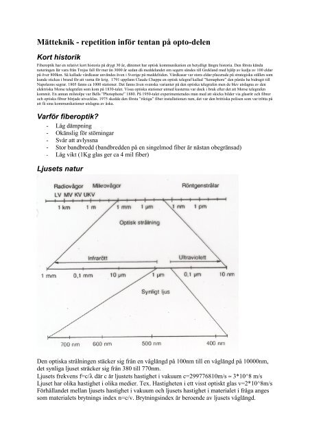
Mätteknik - repetition inför tentan på opto-delen Kort historik Fiberoptik har en relativt kort historia på drygt 30 år, däremot har optisk kommunikation en betydligt längre historia. Den första kända noteringen lär vara från Trojas fall för mer än 3000 år sedan då meddelandet om segern sändes till Grekland med hjälp av kedja av 100 eldar på över 800km. Så kallade vårdkasar användes även i Sverige på meddeltiden. Vårdkasar var stora eldar placerade på strategiska ställen som kunde stickas i brand för att varna för krig. 1791 uppfann Claude Chappe en optisk telegraf kallad ”Semaphore” den påstås ha bidragit till Napoleons segrar. 1805 fanns ca 1000 stationer. Det fanns även svenska varianter på den optiska telegrafen men de blev utslagna av den elektriska Morse telegrafen som kom på 1830-talet. Vissa optiska stationer utmed kusterna var dock i bruk efter det att Morse telegrafen kommit. En annan milstolpe var Bells ”Photophone” 1880. På 1950-talet experimenterades man med att skicka bilder via glasrör och fibrer och optiska fibrer började utvecklas. 1975 skedde den första ”riktiga” fiber installationen rum, det var den brittiska polisen som var trötta på att få sina kommunikationer utslagna av åska. Varför fiberoptik? - Låg dämpning - Okänslig för störningar - Svår att avlyssna - Stor bandbredd (bandbredden på en singelmod fiber är nästan obegränsad) - Låg vikt (1Kg glas ger ca 4 mil fiber) Ljusets natur Den optiska strålningen stäcker sig från en våglängd på 100nm till en våglängd på 10000nm, det synliga ljuset sträcker sig från 380 till 770nm. Ljusets frekvens f=c/λ där c är ljustets hastighet i vakuum c=299776810m/s ≈ 3*10^8 m/s Ljuset har olika hastighet i olika medier. Tex. Hastigheten i ett visst optiskt glas v=2*10^8m/s Förhållandet mellan ljusets hastighet i vakuum och ljusets hastighet i materialet i fråga anges som materialets brytnings index n=c/v. Brytningsindex är beroende av ljusets våglängd.
- Page 2 and 3: Ex. brytningsindex för: Luft 1.0 V
- Page 4 and 5: Dispersion Dispersion - allmänt: s
- Page 6 and 7: Spektrum mätningar Ljuset passerar
- Page 8 and 9: Exinction Ratio ER mäts också ur
- Page 10 and 11: Figure 3. Conduction band and valen
- Page 12 and 13: Figure 6. Illustration of laser his
- Page 14 and 15: The influence of the change in refr
Mätteknik - repetition inför t<strong>en</strong>tan <strong>på</strong> opto-del<strong>en</strong><br />
Kort historik<br />
<strong>Fiberoptik</strong> <strong>har</strong> <strong>en</strong> <strong>relativt</strong> <strong>kort</strong> <strong>historia</strong> <strong>på</strong> <strong>drygt</strong> <strong>30</strong> <strong>år</strong>, <strong>däremot</strong> <strong>har</strong> optisk kommunikation <strong>en</strong> betydligt längre <strong>historia</strong>. D<strong>en</strong> första kända<br />
notering<strong>en</strong> lär vara från Trojas fall för mer än <strong>30</strong>00 <strong>år</strong> sedan då meddelandet om segern sändes till Grekland med hjälp av kedja av 100 eldar<br />
<strong>på</strong> över 800km. Så kallade v<strong>år</strong>dkasar användes äv<strong>en</strong> i Sverige <strong>på</strong> meddeltid<strong>en</strong>. V<strong>år</strong>dkasar var stora eldar placerade <strong>på</strong> strategiska ställ<strong>en</strong> som<br />
kunde stickas i brand för att varna för krig. 1791 uppfann Claude Chappe <strong>en</strong> optisk telegraf kallad ”Semaphore” d<strong>en</strong> <strong>på</strong>stås ha bidragit till<br />
Napoleons segrar. 1805 fanns ca 1000 stationer. Det fanns äv<strong>en</strong> sv<strong>en</strong>ska varianter <strong>på</strong> d<strong>en</strong> optiska telegraf<strong>en</strong> m<strong>en</strong> de blev utslagna av d<strong>en</strong><br />
elektriska Morse telegraf<strong>en</strong> som kom <strong>på</strong> 18<strong>30</strong>-talet. Vissa optiska stationer utmed kusterna var dock i bruk efter det att Morse telegraf<strong>en</strong><br />
kommit. En annan milstolpe var Bells ”Photophone” 1880. På 1950-talet experim<strong>en</strong>terades man med att skicka bilder via glasrör och fibrer<br />
och optiska fibrer började utvecklas. 1975 skedde d<strong>en</strong> första ”riktiga” fiber installation<strong>en</strong> rum, det var d<strong>en</strong> brittiska polis<strong>en</strong> som var trötta <strong>på</strong><br />
att få sina kommunikationer utslagna av åska.<br />
Varför fiberoptik?<br />
- Låg dämpning<br />
- Okänslig för störningar<br />
- Sv<strong>år</strong> att avlyssna<br />
- Stor bandbredd (bandbredd<strong>en</strong> <strong>på</strong> <strong>en</strong> singelmod fiber är nästan obegränsad)<br />
- Låg vikt (1Kg glas ger ca 4 mil fiber)<br />
Ljusets natur<br />
D<strong>en</strong> optiska strålning<strong>en</strong> stäcker sig från <strong>en</strong> våglängd <strong>på</strong> 100nm till <strong>en</strong> våglängd <strong>på</strong> 10000nm,<br />
det synliga ljuset sträcker sig från 380 till 770nm.<br />
Ljusets frekv<strong>en</strong>s f=c/λ där c är ljustets hastighet i vakuum c=299776810m/s ≈ 3*10^8 m/s<br />
Ljuset <strong>har</strong> olika hastighet i olika medier. Tex. Hastighet<strong>en</strong> i ett visst optiskt glas v=2*10^8m/s<br />
Förhållandet mellan ljusets hastighet i vakuum och ljusets hastighet i materialet i fråga anges<br />
som materialets brytnings index n=c/v. Brytningsindex är bero<strong>en</strong>de av ljusets våglängd.
Ex. brytningsindex för: Luft 1.0<br />
Vatt<strong>en</strong> 1.34<br />
Optiskt glas 1.4-1.8<br />
Etanol 1.37<br />
Reflektion och brytning<br />
n1<br />
n2<br />
vi<br />
vr<br />
vb<br />
En ljusstråla g<strong>år</strong> från ett optiskt tätare till ett optiskt tunnare medium n1>n2. Då infallsvinkeln<br />
ökar närmar sig brytningsvinkeln 90°. Om infallsvinkeln ökar ytterligare uppst<strong>år</strong><br />
totalreflektion. Totalreflektion – fysikaliska förutsättning<strong>en</strong> för fiberoptik.<br />
En del av ljuset absorberas – blir värme, ex. En fönsterruta blir inte så varm, det mesta av<br />
ljuset g<strong>år</strong> ig<strong>en</strong>om. En vitt yta blir inte så varm, det mesta ljuset reflekteras. En svart yta blir<br />
varm, ljuset absorberas.<br />
Sinus för d<strong>en</strong> maximala vinkeln som ger upphov till totalreflektion kallas numerisk apertur.<br />
Viktigt när man anger <strong>en</strong> fibers eg<strong>en</strong>skap.<br />
Luft, n=1 n2<br />
x<br />
n1<br />
n2<br />
Ljus som träffar <strong>en</strong> yta med ett annat brytningsindex kan inte helt tränga ig<strong>en</strong>om d<strong>en</strong>na. En<br />
del av ljuset kommer att reflekteras. D<strong>en</strong>na förlust kallas Fresnelförlust.<br />
Fresnelförluster - viktigt att känna till i samband med optiska kontakter.<br />
4%<br />
4%<br />
vi = infallsvinkeln, vr = reflektions vinkeln<br />
vb = brytningsvinkeln<br />
vi = vr<br />
n1*sin(vi) = n2*sin(vb)<br />
Numerisk apertur<br />
NA = sin(x)<br />
NA = (n1^2-n2^2)^(1/2)<br />
F = ((n1-n2)/(n1+n2))^2<br />
ex. glas och luft n1=1.5, n2=1.0<br />
ger F=0.04, dvs 4%.
Förluster i fiber<br />
- Absorption, stör atomer tar upp ljus och bildar värme<br />
- Rayleigh-spridning, reflektion från partiklar och inhomog<strong>en</strong>iteter i materialet.<br />
Proportionell mot 1/λ^4<br />
- Inkopplingsförluster<br />
- Böjförluster<br />
Olika typer av fibrer<br />
- Stegindex, SI (multimod)<br />
- Gradi<strong>en</strong>tindex, G (multimod)<br />
- Singelmod (singelmod)<br />
Det är singelmod som gäller i telekommunikationssystem.<br />
Multimod:<br />
Strålar med många olika<br />
utbredningsvinklar mot<br />
fiber axeln förekommer<br />
Dämpning för <strong>en</strong> fiber visas i figur<strong>en</strong> nedan. Man talar ibland om tre fönster, 1:a fönstret osv.<br />
det är våglängdsområd<strong>en</strong>a runt de tre ljuskällorna, LD.
Dispersion<br />
Dispersion – allmänt: spridning<br />
fiber<br />
Puls in Puls ut<br />
Moddispersion<br />
Spridning i löptid mellan olika moder – uppst<strong>år</strong> i princip bara i multimod fibrer. Olika moder<br />
<strong>har</strong> olika lång transport sträcka.<br />
Materialdispersion<br />
Glasets brytningsindex och därmed ljusets hastighet i fibern ändras med våglängd<strong>en</strong> därför<br />
blir det <strong>en</strong> löptidsvariation mellan de olika våglängderna i ljusets spektrum. Material<br />
dispersion<strong>en</strong> är direkt proportionell mot ljuskällans spektralbredd.<br />
( Vågledardispersion<br />
Vågledardispersion<strong>en</strong> är proportionell mot ljuskällans spektralbredd.)<br />
Kromatisk dispersion<br />
Materialdispersion och vågledardispersion kallas kromatisk dispersion.<br />
Effektmätning<br />
R<br />
Transimpedans LP-filter Voltmeter<br />
förstärkare<br />
Fotodiod<br />
Fotodiodströmm<strong>en</strong> är proportionell mot ljuseffekt<strong>en</strong>. Spänning<strong>en</strong> efter<br />
transimpedansförstärkar<strong>en</strong> är proportionell mot strömm<strong>en</strong>. V = Idiod*R<br />
Lågpassfiltret filtrerar bort högfrekv<strong>en</strong>t brus från transimpedansförstärkar<strong>en</strong>.<br />
Reflex mätningar<br />
Reflex mätningar görs med <strong>en</strong> reflektometer (<strong>en</strong>g. backscatter).<br />
Reflex mätningar görs för att kunna se var fel finns i <strong>en</strong> fiber. Fiberns dämpning kan äv<strong>en</strong><br />
mätas med <strong>en</strong> reflektometer. Dämpning<strong>en</strong> fås av lutning<strong>en</strong> <strong>på</strong> kurvan.
sträckan = hastighet * tid hastighet = c / brytningsindex
Spektrum mätningar<br />
Ljuset passerar g<strong>en</strong>om ett optiskt variabelt bandpass filter kontrollerat av <strong>en</strong> mikroprocessor.<br />
Det återstå<strong>en</strong>de ljuset träffar <strong>en</strong> fotodetektor. Ljus -> Ström -> trans.imp.först.-> spänning.<br />
Våglängd<strong>en</strong> <strong>på</strong> bandpassfiltret och spänning<strong>en</strong> samplas samtidigt.<br />
Bandpass-<br />
Ljus in filter<br />
Kontroll-<br />
Krets<br />
Viktiga parametrar i spektrumet är SMSR, huvudmod<strong>en</strong>s våglängd och huvudmod<strong>en</strong>s effekt.<br />
Våglängds mätning<br />
Samma princip som spektrummätning fast noggrannare. Man är <strong>en</strong>dast intresserad av<br />
huvudmod<strong>en</strong>s våglängd.<br />
V
BER-mätningar<br />
Bit Error Ratio<br />
BER=E(t)/N(t) där E(t) är antalet bitar som är fel<br />
N(t) är antalet mottagna bitar<br />
t kallas gating time – under hur lång tid man räknar mottagna bitar och fel<br />
Pattern g<strong>en</strong>erator - System under test Error detection<br />
mönster g<strong>en</strong>erator kan vara sändare +<br />
ofta PBRS 2^23-1 fiber + mottagare<br />
PBRS – Pseudo Random Binary Sequ<strong>en</strong>ce<br />
Ögondiagram –Eye diagram<br />
Bitström<br />
Effekt ut från lasern<br />
Clock source<br />
Ett ögondiagram ”byggs upp” av ”alla” möjliga kombinationer av bitar. På oscilloskopet som<br />
mäter ögondiagrammet kan man lägga in <strong>en</strong> mask för att trimma in ögondiagrammet och mäta<br />
maskträffar. Ett ”snyggt” ögondiagram utan stora översvängar (overshot) och msakträffar<br />
tyder <strong>på</strong> lite bitfel och att modhopp inte förekommer och att lasern förmodlig<strong>en</strong> <strong>har</strong> ett bra<br />
SMSR värde.<br />
mask<br />
bit period<br />
0 0 0 En 1:a som föregås<br />
0 0 1 av tex två 0:or kanske<br />
0 1 0 inte ser lika dan ut<br />
0 1 1 osv. som <strong>en</strong> 1:a som föregås<br />
1 0 0 av tex <strong>en</strong> 1:a och <strong>en</strong> 0:a<br />
1 0 1<br />
1 1 0<br />
1 1 1<br />
one-level P1<br />
crossing amplitude<br />
zero-level P0
Exinction Ratio ER mäts också ur ögondiagrammet. ER=P1/P0 där P1 är medelvärdet <strong>på</strong><br />
effekt<strong>en</strong> för <strong>en</strong> 1:a och P0 meddelvärdet <strong>på</strong> effekt<strong>en</strong> för <strong>en</strong> 0:a. Maximalt Extincion Ratio är<br />
inte alltid bäst, det innebär att man ”sl<strong>år</strong>” lasern helt av och <strong>på</strong>. (Externt modulerade lasrar<br />
lider inte av detta problem). Optimalt Extinction Ratio då laserns biasström och ”ström för<br />
1:a” är inställd för minsta möjliga bitfel.<br />
Exempel <strong>på</strong> ögondiagram med maskträff och spektrum för samma laser<br />
Exempel <strong>på</strong> ögondiagram med overshot<br />
Lasern<br />
I telekommunikation används halvledarlasrar (laser dioder). Uppbyggnad<strong>en</strong> av <strong>en</strong> modern<br />
halvledarlaser är mycket komplicerad m<strong>en</strong> det kan vara bra att känna till principerna.<br />
Nedanstå<strong>en</strong>de avsnitt är kopierat rakt av från mitt exam<strong>en</strong>sarbete det kan vara bra att skumma<br />
ig<strong>en</strong>om lite snabbt. Lasrar med extern modulator finns inte nämnt det är annars vanligt<br />
förekommande.<br />
-----------------------------------------------------------------------------------------------------------
2. Theory<br />
This chapter includes basic theory about radiative transitions and the semiconductor laser.<br />
It also includes a subsection about spectrum measurem<strong>en</strong>t where parameters in the<br />
frequ<strong>en</strong>cy domain are defined and explained graphically. It finally contains a subsection<br />
about measurem<strong>en</strong>ts that are performed in the production.<br />
2.1 Light-matter interactions<br />
Figure 2. Illustration of emission in a simple atom model, a: Absorption, b: Spontaneous emission, c: Stimulated emission.<br />
Electrons in an atom can be excited to a higher <strong>en</strong>ergy state in many differ<strong>en</strong>t ways, one<br />
of them is by <strong>en</strong>ergy of light. The <strong>en</strong>ergy can cause an electron in a lower <strong>en</strong>ergy level to<br />
jump to a level of higher <strong>en</strong>ergy. Wh<strong>en</strong> dealing with absorption and g<strong>en</strong>eration of light<br />
three important processes occur.<br />
In figure 2a, the electron is at its regular stable state, and an incoming photon makes the<br />
electron jump to a level with higher <strong>en</strong>ergy. The atom is now excited. This procedure is<br />
called absorption.<br />
Wh<strong>en</strong> the electron is in a level of higher <strong>en</strong>ergy it might jump back to a level of lower<br />
<strong>en</strong>ergy and a photon is transmitted. This is called spontaneous emission, since this<br />
process occurs without external influ<strong>en</strong>ce. This is illustrated in figure 2b.<br />
In figure 2c, an incoming photon makes the electron in the higher <strong>en</strong>ergy level jump<br />
down and another photon with the same wavel<strong>en</strong>gth and phase as the incoming photon<br />
leaves the atom. This is called stimulated emission.<br />
The abbreviation laser stands for light amplification by stimulated emission of radiation.<br />
4
Figure 3. Conduction band and val<strong>en</strong>ce band for an isolator, semiconductor, and a conductor<br />
In a solid material the electron’s <strong>en</strong>ergy levels will interact with each other and several<br />
levels will appear. For example: if two atoms are brought together, two <strong>en</strong>ergy levels will<br />
correspond to every <strong>en</strong>ergy level before they were brought together. In a solid material<br />
these several <strong>en</strong>ergy levels form a band. Electrons can only have <strong>en</strong>ergy within one of the<br />
bands and not in the bandgap, see figure 3. The upper band is called the conduction band<br />
and the lower band is called the val<strong>en</strong>ce band. Materials with a bandgap of typically 1eV<br />
have suffici<strong>en</strong>t numbers of free electrons to conduct electrical curr<strong>en</strong>t at room<br />
temperature. Such materials are called semiconductors. In metals, the val<strong>en</strong>ce band and<br />
the conduction band overlap and therefor there is no bandgap. This is the reason why<br />
metals are good conductors. Isolators have a bandgap of approximately 5eV or more. The<br />
photons that are transmitted have a wavel<strong>en</strong>gth λ.<br />
λ = h * c / Eg (1)<br />
where: h is Plancks constant, h=4.1*10^-15 [eVs]<br />
c is the speed of light in vacuum, c=3*10^8 [m/s]<br />
Eg is the <strong>en</strong>ergy of the bandgap [eV]<br />
Eg=Ec-Ev (2)<br />
where: Ec is the lowest <strong>en</strong>ergy of the conduction band [eV]<br />
Ev is the highest <strong>en</strong>ergy of the val<strong>en</strong>ce band [eV]<br />
The electrons and holes in the conduction- and val<strong>en</strong>ce band are oft<strong>en</strong> assumed to have a<br />
Fermi-Dirac distribution. For more theory on radiative transitions see Tell, Andersson,<br />
Andersson[3], Milloni, Eberly[4] and Nilsson-Gistvik[5].<br />
2.2 Semiconductor DFB laser<br />
The light-matter interactions that were described in the previous chapter take place in the<br />
optical cavity of the laser. The semiconductor laser is electrically “pumped” to inject<br />
electrons and holes and to get stimulated emission. The simplest way to achieve a cavity<br />
is to cleave the two sides perp<strong>en</strong>dicular to the PN-junction to get two parallel semi-<br />
5
transpar<strong>en</strong>t facets. This structure is called a Fabry-Perot cavity. Only the photons which<br />
have an integer number of half wavel<strong>en</strong>gths that corresponds to the l<strong>en</strong>gth of the cavity is<br />
amplified, other wavel<strong>en</strong>gths will be att<strong>en</strong>uated, see figure 4.<br />
Figure 4. Fabry-Perot cavity, k is an integer number.<br />
The stimulated emission, or “lasing”, arises wh<strong>en</strong> a threshold in the driving curr<strong>en</strong>t is<br />
reached. Figure 5 shows the output power for a laser-diode and a LED (Light emitting<br />
diode) respectively. Wh<strong>en</strong> measuring an IP-curve the threshold curr<strong>en</strong>t is defined as the<br />
curr<strong>en</strong>t at the maximum second derivative of output power against curr<strong>en</strong>t.<br />
Figure 5. Output power as a function of driving curr<strong>en</strong>t for a laser-diode and a LED, IP-curve.<br />
The first manufactured lasers just worked for a few seconds in extremely low<br />
temperatures, see figure 6a. To improve the lasers an active layer of another material was<br />
put betwe<strong>en</strong> the PN-junction, see figure 6b. Later the active layer was buried and<br />
consisted of a very thin stripe, see figure 6c.<br />
6
Figure 6. Illustration of laser history. a: The first laser, b: An active layer is introduced, c: The active layer is buried.<br />
The laser structure with an active layer of an another material showed in figure 6b and 6c<br />
is called double heterojunction structure. Figure 7 shows the PN-junction diagram for a<br />
homojunction and a double heterojunction laser.<br />
Figure 7. PN-junctions for a: Homojunction laser, b: Double heterojunction laser.<br />
DFB is an abbreviation for Distributed Feedback. The idea of a DFB laser is to introduce<br />
a grating over the active layer. The grating will act like a band-pass filter and only the<br />
wavel<strong>en</strong>gths that correspond to the distance betwe<strong>en</strong> the grating lines will be gained. The<br />
DFB laser has a much narrower spectrum th<strong>en</strong> the Fabry-Perot laser. Figure 8 shows the<br />
structure and spectrum for the Fabry-Perot and the DFB laser, respectively.<br />
7
Figure 8. structure and spectrum for the Fabry-Perot and the DFB laser, respectively.<br />
The figures above just show the principal structures of lasers. The lasers that are actually<br />
used are more complicated. The active layer in the laser chip that is used in the submodule<br />
consists of several very thin layers. This structure is called MQW, which is an<br />
abbreviation for multiple quantum wells. The thin layers of the MQW structure make the<br />
material to be strained. Strained materials reduce the influ<strong>en</strong>ce of so called light and<br />
heavy holes, LH and HH.<br />
For more about semiconductor lasers see Milloni, Eberly[4], Nilsson-Gistvik[5], Buus[9]<br />
and Coldr<strong>en</strong>, Corzine[10].<br />
2.3 SMSR<br />
SMSR is an abbreviation for side mode suppression ratio as m<strong>en</strong>tioned before. The<br />
definition of SMSR is the differ<strong>en</strong>ce in amplitude betwe<strong>en</strong> the main mode and the largest<br />
side mode. SMSR is an effect of several parameters. The l<strong>en</strong>gth of the laser cavity is<br />
dep<strong>en</strong>d<strong>en</strong>t on temperature, most materials expands wh<strong>en</strong> temperature is increasing, this is<br />
also the case for the laser cavity. Wh<strong>en</strong> the l<strong>en</strong>gth of the cavity increases another<br />
wavel<strong>en</strong>gth can be amplified.<br />
L = λ/2 * k � λ = 2 * L/k (3)<br />
where: k is an integer number.<br />
L is the l<strong>en</strong>gth of the laser cavity.<br />
The distance betwe<strong>en</strong> the grating lines in the DFB-grating will also be affected by<br />
temperature in a similar way. Wh<strong>en</strong> modulating the laser voltage the carrier d<strong>en</strong>sity<br />
changes and this makes the refractive index n in the laser cavity change and the change in<br />
refractive index causes the wavel<strong>en</strong>gth to change.<br />
λ = 2 * L* n/k (4)<br />
8
The influ<strong>en</strong>ce of the change in refractive index increases with increasing modulation<br />
frequ<strong>en</strong>cy. The refractive index is also dep<strong>en</strong>d<strong>en</strong>t on the wavel<strong>en</strong>gth. Equation (4) states<br />
that the wavel<strong>en</strong>gth increases wh<strong>en</strong> the refractive index increases. The laser curr<strong>en</strong>t does<br />
also effect the SMSR. The electrons and holes in the conduction and val<strong>en</strong>ce band have a<br />
Fermi-Dirac distribution, see section 2.1. Figure 9 shows a principal figure of this.<br />
Figure 9. Distribution of electrons and holes in conduction- and val<strong>en</strong>ce bands.<br />
The mean <strong>en</strong>ergy in figure 9 gives the c<strong>en</strong>ter wavel<strong>en</strong>gth of the lasers gain curve. Wh<strong>en</strong><br />
the laser is pumped with a low curr<strong>en</strong>t, only the inner part of the distribution is filled with<br />
electrons and holes, i.e. the dark gray area in figure 9. Wh<strong>en</strong> the laser is pumped with<br />
higher curr<strong>en</strong>ts the electrons and holes fill up more of the distribution and the mean<br />
<strong>en</strong>ergy will increase. Formula (1) in section 2.1 gives that this makes the wavel<strong>en</strong>gth<br />
decrease. Figure 10 shows how the gain curve of the laser and the l<strong>en</strong>gth of the laser<br />
cavity affects the spectrum.<br />
Figure 10. The drift in wavel<strong>en</strong>gth of the lasers gain curve and the modes possible in the cavity.<br />
9
The gain curve of the laser and the possible modes pres<strong>en</strong>t in the laser cavity can drift in<br />
wavel<strong>en</strong>gth with temperature and degradation. This can cause mode-jumps to occur, see<br />
Tell, Andersson, Andersson[3] and Buus[9] for more information.<br />
2.4 Spectrum measurem<strong>en</strong>t<br />
This chapter includes a subsection about the spectrum analyzer and how it work. It also<br />
includes a subsection with definitions of parameters that are measured in frequ<strong>en</strong>cy<br />
domain. For more information about spectrum measurem<strong>en</strong>ts that are not included in this<br />
chapter see Derickson[1].<br />
2.4.1 The spectrum analyzer<br />
The principle of a spectrum analyzer is that: The light passes through a optical variable<br />
bandpass filter controlled by a microprocessor, and th<strong>en</strong> the remaining light hits a<br />
photodetector that converts the light to curr<strong>en</strong>t. The curr<strong>en</strong>t that is proportional to the<br />
light is th<strong>en</strong> converted to voltage. The wavel<strong>en</strong>gth of the bandpass filter and the voltage<br />
are sampled at the same time.<br />
There are several types of optical spectrum analyzers such as Fabry-Perot-interferometer<br />
based, Michelson-interferometer based, and diffraction based optical spectrum analyzers.<br />
For more information see Derickson[1].<br />
2.4.2 Frequ<strong>en</strong>tly used definitions<br />
Apart from SMSR some other parameters in the frequ<strong>en</strong>cy domain are oft<strong>en</strong> measured.<br />
The following definitions are frequ<strong>en</strong>tly used.<br />
SMSR (Side mode suppression ratio): The differ<strong>en</strong>ce in amplitude betwe<strong>en</strong> the main<br />
mode and the largest side mode.<br />
Peak amplitude: The power of the main mode.<br />
Peak wavel<strong>en</strong>gth: The wavel<strong>en</strong>gth where the main mode occurs.<br />
Mode offset: The distance betwe<strong>en</strong> the wavel<strong>en</strong>gth of the main mode and the SMSR<br />
mode.<br />
Stopband: The distance betwe<strong>en</strong> the left and right side mode adjac<strong>en</strong>t to the main mode.<br />
Bandwidth: The bandwidth of the main mode The amplitude level relative to the peak<br />
amplitude is oft<strong>en</strong> chos<strong>en</strong> to –20dB for a DFB-laser.<br />
These definitions and especially the definition of SMSR, which is frequ<strong>en</strong>tly used in this<br />
thesis, are graphically explained in figure 11.<br />
10


