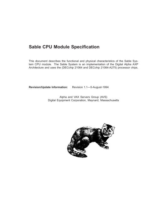
Sable CPU Module Specification
Sable CPU Module Specification
Sable CPU Module Specification

Create successful ePaper yourself
Turn your PDF publications into a flip-book with our unique Google optimized e-Paper software.
<strong>Sable</strong> <strong>CPU</strong> <strong>Module</strong> <strong>Specification</strong><br />
This document describes the functional and physical characteristics of the <strong>Sable</strong> System<br />
<strong>CPU</strong> module. The <strong>Sable</strong> System is an implementation of the Digital Alpha AXP<br />
Architecture and uses the (DECchip 21064 and DECchip 21064-A275) processor chips.<br />
Revision/Update Information: Revision 1.1—5-August-1994<br />
KURT M. THALLER (TBONE::THALLER, 223-4599)<br />
Alpha and VAX Servers Group (AVS)<br />
Digital Equipment Corporation, Maynard, Massachusetts
Digital Equipment Corporation makes no representations that the use of its products in the manner described<br />
in this publication will not infringe on existing or future patent rights, nor do the descriptions contained<br />
in this publication imply the granting of licenses to make, use, or sell equipment or software in accordance<br />
with the description.<br />
The information in this document is subject to change without notice and should not be construed as a commitment<br />
by Digital Equipment Corporation.<br />
Digital Equipment Corporation assumes no responsibility for any errors that may appear in this document.<br />
The software, if any, described in this document is furnished under a license and may be used or copied only<br />
in accordance with the terms of such license. No responsibility is assumed for the use or reliability of software<br />
or equipment that is not supplied by Digital Equipment Corporation or its affiliated companies.<br />
Copyright © 1990−1994 by Digital Equipment Corporation.<br />
All Rights Reserved.<br />
Printed in U.S.A.<br />
The following are trademarks of Digital Equipment Corporation: AlphaServer, DEC LANcontroller,<br />
OpenVMS, StorageWorks, VAX, and the DIGITAL logo.<br />
MEMORY CHANNEL is a trademark of Encore Computer Corporation.<br />
FCC NOTICE: The equipment described in this manual generates, uses, and may emit radio frequency energy.<br />
The equipment has been type tested and found to comply with the limits for a Class A computing device<br />
pursuant to Subpart J of Part 15 of FCC Rules, which are designed to provide reasonable protection<br />
against such radio frequency interference when operated in a commercial environment. Operation of this<br />
equipment in a residential area may cause interference, in which case the user at his own expense may be<br />
required to take measures to correct the interference.
CONTENTS<br />
Preface ........................................................ v<br />
Chapter 1 <strong>CPU</strong> MODULE COMPONENTS AND FEATURES .......... 1<br />
1.1 The 21064 <strong>CPU</strong> Chip ........................................... 4<br />
1.2 The Alpha AXP Architecture . . ................................... 5<br />
Chapter 2 <strong>CPU</strong> MODULE VARIATIONS ............................. 7<br />
2.1 Form Factors ................................................. 7<br />
Chapter 3 FUNCTIONS LOCATED ON THE DECCHIP 21064 ......... 9<br />
3.1 21064 Chip Features . ........................................... 9<br />
3.1.1 I-box Internal Processor Registers ............................... 11<br />
3.1.2 Branch Prediction Logic . . . ................................... 11<br />
3.1.3 Instruction Translation Buffers (ITBs) . .......................... 12<br />
3.1.4 Interrupt Logic . . ........................................... 13<br />
3.1.5 Performance Counters ........................................ 14<br />
3.1.6 Translation Buffer Tag Register (TB_TAG) ........................ 16<br />
3.1.7 Instruction Translation Buffer Page Table Entry Register (ITB_PTE) . . . . 18<br />
3.1.8 Instruction Cache Control and Status Register (ICCSR) .............. 19<br />
3.1.9 Instruction Translation BUffer Page Table Entry Temporary<br />
Register(ITB_PTE_TEMP) .................................... 21<br />
3.1.10 Exception Address Register (EXC_ADDR) ........................ 21<br />
3.1.11 Serial Line Clear Register (SL_CLR) . . .......................... 23<br />
3.1.12 Serial Line Receive Register (SL_RCV) .......................... 23<br />
3.1.13 Instruction Translation Buffer Zap Register (ITBZAP) .............. 24<br />
3.1.14 Instruction Translation Buffer ASM Register (ITBASM) . . .......... 24<br />
3.1.15 Instruction Translation Buffer IS Register (ITBIS) ................. 24<br />
3.1.16 Processor Status (PS) ....................................... 25<br />
3.1.17 Exception Summary Register (EXC_SUM) ....................... 26<br />
3.1.18 Privileged Architecture Library Base Register (PAL_BASE) .......... 28<br />
3.1.19 Hardware Interrupt Request Register (HIRR) . . .................. 29<br />
3.1.20 Software Interrupt Request Register (SIRR) . . . .................. 31<br />
3.1.21 Asynchronous Trap Request Register (ASTRR) . . .................. 32<br />
3.1.22 Hardware Interrupt Enable Register (HIER) . . . .................. 33<br />
3.1.23 Software Interrupt Enable Register (SIER) ...................... 34<br />
3.1.24 Asynchronous System Trap Enable Register (ASTER) .............. 35<br />
3.1.25 Serial Line Transmit (SL_XMIT) .............................. 36<br />
3.2 Ebox ........................................................ 37<br />
3.3 Abox ........................................................ 37<br />
iii
iv<br />
3.3.1 Abox IPRs ................................................. 37<br />
3.3.2 Translation Buffer Control Register (TB_CTL) . . . .................. 38<br />
3.3.3 Data Translation Buffer Page Table Entry Register (DTB_PTE) ....... 39<br />
3.3.4 Data Translation Buffer Page Table Entry Temporary Register<br />
(DTB_PTE_TEMP) .......................................... 40<br />
3.3.5 Memory Management Control and Status Register (MM_CSR) ........ 41<br />
3.3.6 Virtual Address Register (VA) .................................. 41<br />
3.3.7 Data Translation Buffer Zap Register (DTBZAP) . .................. 41<br />
3.3.8 Data Translation Buffer ASM Register (DTBASM) ................. 42<br />
3.3.9 Data Translation Buffer Invalidate Signal Register (DTBIS) .......... 42<br />
3.3.10 Flush Instruction Cache Register (FLUSH_IC) . .................. 42<br />
3.3.11 Flush Instruction Cache ASM Register (FLUSH_IC_ASM) . .......... 42<br />
3.3.12 A-box Control Register (ABOX_CTL) . .......................... 42<br />
3.3.13 Alternative Processor Mode Register (ALT_MODE) ................ 46<br />
3.3.14 Cycle Counter Register (CC) .................................. 46<br />
3.3.15 Cycle Counter Control Register (CC_CTL) ....................... 46<br />
3.3.16 Bus Interface Unit Control Register (BIU_CTL) . .................. 46<br />
3.3.17 Data Translation Buffer (DTB) ................................ 53<br />
3.3.18 Bus Interface Unit (BIU) . . ................................... 54<br />
3.3.19 Load Silos ................................................ 54<br />
3.3.20 Write Buffer ............................................... 55<br />
3.4 Fbox ........................................................ 56<br />
3.5 21064 IEEE Floating Point Conformance . . .......................... 57<br />
3.6 Cache Organization . ........................................... 59<br />
3.6.1 Data Cache (Dcache) ......................................... 59<br />
3.6.2 Instruction Cache (Icache) . . ................................... 59<br />
3.7 Pipeline Organization ........................................... 59<br />
3.7.1 Static and Dynamic Stages . ................................... 61<br />
3.7.2 Aborts . ................................................... 61<br />
3.7.3 Non-Issue Conditions ......................................... 63<br />
3.8 Scheduling and Issuing Rules . . ................................... 63<br />
3.8.1 Instruction Class Definition . ................................... 63<br />
3.8.2 Producer-Consumer Latency ................................... 65<br />
3.8.3 Producer-Producer Latency . ................................... 67<br />
3.8.4 Instruction Issue Rules ....................................... 67<br />
3.8.5 Dual Issue Table . ........................................... 68<br />
3.9 PALcode . . ................................................... 69<br />
3.9.1 Required PALcode Instructions ................................. 70<br />
3.9.2 Architecturally Reserved PALcode Instructions . . . .................. 70<br />
3.9.3 PAL_TEMPs ............................................... 70<br />
3.9.4 Data Cache Status Register (C_STAT) . .......................... 70<br />
3.9.5 DECchip 21064-A275 Data Cache Status Register (C_STAT) .......... 71
3.9.6 Data Cache Address Register (DC_ADDR) ........................ 73<br />
3.9.7 Bus Interface Unit Status Register (BIU_STAT) . .................. 74<br />
3.9.8 Bus Interface Unit Address Register (BIU_ADDR) .................. 75<br />
3.9.9 Fill Address Register (FILL_ADDR) . . . .......................... 77<br />
3.9.10 Fill Syndrome Register (FILL_SYNDROME) . . . .................. 78<br />
3.9.11 Backup Cache Tag Register (BC_TAG) . .......................... 79<br />
3.9.12 EDC Error Correction ....................................... 81<br />
Chapter 4 FUNCTIONS LOCATED ELSEWHERE ON THE <strong>CPU</strong><br />
MODULE ...................................................... 83<br />
4.1 Back-up Cache (B-Cache) ........................................ 83<br />
4.1.1 Control Store ............................................... 83<br />
4.1.2 Tag Store .................................................. 84<br />
4.1.3 Data Store ................................................. 84<br />
4.1.4 B-Cache Control Register Definitions . . .......................... 85<br />
4.1.4.1 CSR Space . . . ........................................... 85<br />
4.1.4.2 B-Cache Control Register - CSR0 . . . .......................... 86<br />
4.1.4.3 B-Cache Correctable Error Register - CSR1 . . . .................. 92<br />
4.1.4.4 B-Cache Correctable Error Address Register - CSR2 .............. 95<br />
4.1.4.5 B-Cache Uncorrectable Error Register - CSR3 . .................. 97<br />
4.1.4.6 B-Cache Uncorrectable Error Address Register - CSR4 . . .......... 100<br />
4.1.5 Back-up Cache Cycle Time . ................................... 101<br />
4.1.5.1 The 21064 Cycles ......................................... 102<br />
4.1.5.2 System-bus Cycles ........................................ 102<br />
4.2 Cache Block Merge Buffer ....................................... 102<br />
4.3 Duplicate Primary Data Cache Tag Store . . .......................... 103<br />
4.3.1 Duplicate Tag Error Register - CSR5 . . . .......................... 105<br />
4.4 Lack of Duplicate Primary Instruction Cache Tag Store ................. 106<br />
4.5 Lack of Cache Block Prefetch . . ................................... 107<br />
4.6 Data Integrity ................................................. 107<br />
4.7 System-bus Interface ........................................... 107<br />
4.7.1 System-bus Control Register - CSR6 . . . .......................... 108<br />
4.7.2 System-bus Error Register - CSR7 .............................. 111<br />
4.7.3 System-bus Error Address Low Register - CSR8 . . .................. 117<br />
4.7.4 System-bus Error Address High Register - CSR9 . .................. 118<br />
4.8 Multiprocessor Configuration CSR Definitions ........................ 121<br />
4.8.1 Processor Mailbox Register - CSR10 . . . .......................... 121<br />
4.8.2 Interprocessor Interrupt Request Register - CSR11 .................. 122<br />
4.9 System Interrupt Clear Register - CSR12 . . .......................... 123<br />
4.10 Address Lock Register - CSR13 .................................. 125<br />
v
4.11 Miss Address Register - CSR14 ................................... 127<br />
4.11.1 C4 Revision Register - CSR15 ................................. 128<br />
4.12 Interval Timer ............................................... 130<br />
4.13 D-bus . . . ................................................... 131<br />
4.14 System-bus Arbiter . ........................................... 133<br />
4.15 System-bus CRESET L Generation ................................ 136<br />
4.15.1 <strong>Sable</strong> <strong>CPU</strong> Non-Volatile EEPROM .............................. 137<br />
Chapter 5 <strong>CPU</strong> MODULE TRANSACTIONS ......................... 143<br />
5.1 Processor Transactions .......................................... 143<br />
5.1.1 21064 Processor TRANSACTIONS .............................. 146<br />
5.1.1.1 FAST EXTERNAL CACHE READ HIT ........................ 146<br />
5.1.1.2 FAST EXTERNAL CACHE WRITE HIT ....................... 147<br />
5.1.1.3 READ_BLOCK TRANSACTION .............................. 148<br />
5.1.1.4 WRITE_BLOCK .......................................... 150<br />
5.1.1.5 LDxL TRANSACTION . . ................................... 152<br />
5.1.1.6 StxC TRANSACTION . . . ................................... 152<br />
5.1.1.7 BARRIER TRANSACTION .................................. 153<br />
5.1.1.8 FETCH TRANSACTION ................................... 153<br />
5.1.1.9 FETCHM TRANSACTION .................................. 154<br />
5.1.2 Cacheable vs Non-Cacheable vs Allocate-Invalid . .................. 155<br />
5.2 System-bus Transactions ........................................ 156<br />
5.2.1 <strong>CPU</strong> as Commander ......................................... 157<br />
5.2.2 <strong>CPU</strong> as Bystander ........................................... 157<br />
5.2.3 <strong>CPU</strong> as Responder ........................................... 157<br />
5.3 Control Flow of <strong>CPU</strong> <strong>Module</strong> Transactions . .......................... 158<br />
5.3.1 Processor Initiated ........................................... 158<br />
5.3.2 System-bus Initiated ......................................... 162<br />
Chapter 6 CACHE INVALIDATE MANAGEMENT .................... 165<br />
6.1 Processor Caused Invalidates . . ................................... 165<br />
6.2 C-bus Caused Invalidates ........................................ 165<br />
Chapter 7 EXCEPTIONS AND INTERRUPTS ........................ 167<br />
vi<br />
7.1 Processor Generated . ........................................... 167
7.1.1 Exception Handling .......................................... 168<br />
7.1.1.1 PAL Priority Level ........................................ 169<br />
7.1.1.2 PALcode 0020 Entry Characteristics .......................... 169<br />
7.1.1.3 PAL Routine Behavior . . ................................... 169<br />
7.1.1.3.1 B-Cache Tag Parity Error ................................ 169<br />
7.1.1.3.2 B-Cache Tag Control Parity Error .......................... 170<br />
7.1.1.3.3 B-Cache Data Single Bit EDC Error ........................ 170<br />
7.1.1.3.4 B-Cache Data Uncorrectable EDC Error . . . .................. 170<br />
7.1.1.3.5 B-Cache Data Single Bit EDC Error ........................ 171<br />
7.1.1.3.6 B-Cache Data Uncorrectable EDC Error . . . .................. 171<br />
7.1.1.3.7 21064 Data bus Single Bit EDC Error ....................... 171<br />
7.1.1.3.8 21064 Data bus Uncorrectable EDC Error . .................. 171<br />
7.1.1.3.9 B-Cache Tag or Tag Control Parity Error . . .................. 172<br />
7.1.1.3.10 Cobra-bus Parity Error ................................. 172<br />
7.1.1.3.11 Invalid Cobra-bus Address ............................... 172<br />
7.1.1.3.12 Other <strong>CPU</strong> Errors . . ................................... 173<br />
7.1.1.3.13 Main Memory Uncorrectable EDC Errors . .................. 173<br />
7.2 Non-processor Generated ........................................ 173<br />
7.2.1 Interrupt Handling .......................................... 173<br />
7.2.1.1 PAL Priority Level ........................................ 174<br />
7.2.1.2 PALcode 00E0 Entry Characteristics .......................... 174<br />
7.2.1.3 Hardware 0 - Hardware Error ............................... 175<br />
7.2.1.4 Hardware 1 - Local I/O . . ................................... 177<br />
7.2.1.5 Hardware 3 - Interprocessor ................................. 177<br />
7.2.1.6 Hardware 4 - Interval Timer ................................ 177<br />
7.2.1.7 Hardware 5 - System Events ................................ 177<br />
7.2.1.8 Software X . . . ........................................... 178<br />
7.2.1.9 Serial Line . . . ........................................... 178<br />
7.2.1.10 Performance Counter X ................................... 178<br />
7.2.1.11 Asynchronous System Trap ................................. 178<br />
Chapter 8 FAULT MANAGEMENT/ERROR RECOVERY .............. 179<br />
8.1 Processor Errors ............................................... 179<br />
8.2 B-Cache Errors ................................................ 179<br />
8.2.1 Tag and Tag Control Store Parity Errors .......................... 179<br />
8.2.2 Data Store EDC Errors ....................................... 181<br />
8.2.2.1 Correctable . . . ........................................... 181<br />
8.2.2.2 Uncorrectable . ........................................... 183<br />
8.3 Duplicate P-Cache Tag Store Parity Errors .......................... 186<br />
8.4 System-bus Errors . . ........................................... 186<br />
8.4.1 C/A Parity Error . ........................................... 186<br />
8.4.2 Data Parity Error ........................................... 187<br />
vii
8.4.3 Invalid Address - Bus Time-out ................................. 187<br />
8.5 I/O Subsystem Errors ........................................... 188<br />
8.6 C_ERR L Assertion . . ........................................... 188<br />
Chapter 9 <strong>CPU</strong> POWERUP AND INITIALIZATION ................... 189<br />
9.1 Processor Initialization .......................................... 189<br />
9.1.1 Internal Processor Registers ................................... 189<br />
9.1.2 Internal JSR stack ........................................... 189<br />
9.2 B-Cache Initialization ........................................... 189<br />
9.2.1 LDQ Data Format - BCC ENABLE B-CACHE INIT Set .............. 190<br />
9.3 Duplicate Tag Store Initialization .................................. 191<br />
9.4 System-bus Interface Initialization ................................. 191<br />
9.5 <strong>CPU</strong> clocks and reset ........................................... 191<br />
9.6 Power-up Sequence . . ........................................... 191<br />
9.7 Powering Up with Bad Main Memory ............................... 192<br />
Chapter 10 OVERVIEW OF THE <strong>CPU</strong> TESTABILITY FEATURES ...... 193<br />
10.1 Bus Verification ............................................... 193<br />
10.1.1 Address .................................................. 193<br />
10.1.2 Data . . ................................................... 193<br />
10.2 C4 EDC Generators ........................................... 193<br />
10.3 C4 EDC Checkers . . ........................................... 194<br />
10.4 DECchip 21064 EDC Checkers ................................... 194<br />
10.5 DECchip 21064 EDC Generators ................................. 194<br />
10.6 C4 Cobra-bus Probe Predicted Tag Parity Generator .................. 194<br />
10.7 B-Cache Data Store Verification .................................. 194<br />
10.8 B-Cache Tag/Control Store Verification . . . .......................... 194<br />
10.9 Performance Counters ......................................... 195<br />
10.10 Brain Dead <strong>Module</strong> Errors . . ................................... 195<br />
Chapter 11 PHYSICAL AND ELECTRICAL CHARACTERISTICS ...... 197<br />
viii<br />
11.1 <strong>CPU</strong> <strong>Module</strong> Physical <strong>Specification</strong> ................................ 197<br />
11.2 SABLE <strong>CPU</strong> CONNECTOR PINNING . . . .......................... 197<br />
11.3 <strong>CPU</strong> <strong>Module</strong> Max DC Power Requirement .......................... 203
11.4 Environmental <strong>Specification</strong>s - Class B modified . . . .................. 203<br />
11.4.1 Temperature . . . ........................................... 203<br />
11.4.1.1 Storage ................................................ 203<br />
11.4.1.2 Operating . . . ........................................... 203<br />
11.4.2 Relative Humidity .......................................... 203<br />
11.4.2.1 Storage ................................................ 204<br />
11.4.2.2 Operating . . . ........................................... 204<br />
11.4.3 Altitude .................................................. 204<br />
11.4.3.1 Storage ................................................ 204<br />
11.4.3.2 Operating Altitude ....................................... 204<br />
11.4.4 Airflow ................................................... 204<br />
11.4.5 Contamination . . ........................................... 204<br />
11.4.6 Mean Time Between Failure (MTBF) Rate ....................... 204<br />
11.4.7 Electrical Characteristics . . ................................... 204<br />
11.4.7.1 AC References ........................................... 204<br />
11.4.8 Clock Description ........................................... 204<br />
11.4.9 AC and DC Characteristics ................................... 208<br />
Appendix A ALPHA ARCHITECTURE OPTIONS SUPPORTED ....... 211<br />
Appendix B SABLE <strong>CPU</strong> MODULE REGISTER REFERENCE GUIDE<br />
............................................................... 213<br />
Appendix C COBRA SPECIFIC ( PRIVILEGED ARCHITECTURE<br />
LIBRARY CODE ) PALCODE .................................... 223<br />
C.1 Introduction .................................................. 223<br />
C.2 PAL Environment . . ........................................... 223<br />
C.3 Special PAL Instructions ........................................ 224<br />
C.3.1 HW_MFPR and HW_MTPR ................................... 225<br />
C.3.2 HW_LD and HW_ST ......................................... 227<br />
C.3.3 HW_REI .................................................. 228<br />
C.4 PAL Entry Points . . . ........................................... 228<br />
C.5 General PALmode Restrictions ................................... 231<br />
C.5.1 21064 PAL Restrictions ....................................... 231<br />
C.5.2 21064 Specific PALmode Restrictions . .......................... 234<br />
C.6 Powerup . . ................................................... 235<br />
C.7 TB Miss Flows ................................................ 237<br />
C.7.1 ITB Miss .................................................. 237<br />
C.7.2 DTB Miss ................................................. 238<br />
C.8 Error Flows .................................................. 239<br />
ix
C.8.1 21064 Error Flows .......................................... 239<br />
C.8.1.1 EDC Error Handling . . . ................................... 239<br />
C.8.1.1.1 Single Bit I-stream EDC error . . .......................... 239<br />
C.8.1.1.2 Single Bit D-stream EDC error . . .......................... 240<br />
C.8.1.1.3 Double Bit I-stream EDC error . . .......................... 240<br />
C.8.1.1.4 Double Bit D-stream EDC error . .......................... 240<br />
C.8.1.2 BIU: tag address parity error ................................ 241<br />
C.8.1.3 BIU: tag control parity error ................................ 241<br />
C.8.1.4 BIU: system transaction terminated with CACK_HERR . .......... 241<br />
C.8.2 Response to Multiple Errors ................................... 241<br />
Appendix D REVISION HISTORY .................................. 243<br />
INDEX<br />
EXAMPLES<br />
1 Update vs Invalidate Algorithm ................................ 104<br />
FIGURES<br />
1 <strong>Sable</strong> <strong>CPU</strong> <strong>Module</strong> Block Diagram .............................. 2<br />
2 C4 Chip Block Diagram ....................................... 3<br />
3 21064 <strong>CPU</strong> Chip Block Diagram ................................ 4<br />
4 <strong>CPU</strong> Form Factors .......................................... 8<br />
5 TB_TAG_FIG ............................................... 17<br />
6 ITB_PTE .................................................. 18<br />
7 ICCSR . ................................................... 19<br />
8 ITB_PTE_TEMP . ........................................... 21<br />
9 EXC_ADDR ................................................ 22<br />
10 SL_CLR ................................................... 23<br />
11 SL_RCV ................................................... 24<br />
12 PS ....................................................... 25<br />
13 EXC_SUM ................................................. 26<br />
14 PAL_BASE ................................................ 28<br />
15 HIRR . . ................................................... 29<br />
16 SIRR . . ................................................... 31<br />
17 ASTRR ................................................... 32<br />
18 HIER . . ................................................... 33<br />
19 SIER . . ................................................... 34<br />
20 ASTER ................................................... 35<br />
21 SL_XMIT .................................................. 36<br />
22 TB_CTL_FIG ............................................... 38<br />
23 DTB_PTE ................................................. 39<br />
24 DTB_PTE_TEMP ........................................... 40<br />
x
25 MM_CSR .................................................. 41<br />
26 DECchip 21064 ABOX_CTL ................................... 43<br />
27 DECchip 21064-A275 ABOX_CTL ............................... 44<br />
28 ALT_MODE ................................................ 46<br />
29 BIU Control Register (BIU_CTL) ............................... 47<br />
30 DECchip 21064-A275 BIU Control Register (EV45_BIU_CTL) ......... 50<br />
31 Integer Operate Pipeline . . . ................................... 60<br />
32 Memory Reference Pipeline . ................................... 60<br />
33 Floating Point Operate Pipeline ................................ 61<br />
34 Producer-Consumer Latency Matrix . . . .......................... 66<br />
35 DECchip 21064 C_STAT . . . ................................... 71<br />
36 DECchip 21064-A275 C_STAT .................................. 71<br />
37 BIU_STAT ................................................. 74<br />
38 Fill Syndrome . . . ........................................... 78<br />
39 BC_TAG .................................................. 80<br />
40 Back-up Cache Entry ........................................ 83<br />
41 B-Cache Control Register (BCC) ................................ 87<br />
42 B-Cache Correctable Error Register (BCCE) ....................... 92<br />
43 B-Cache Correctable Error Address Register (BCCEA) ............... 95<br />
44 B-Cache Uncorrectable Error Register (BCUE) . . . .................. 97<br />
45 B-Cache Uncorrectable Error Address Register (BCUEA) . . . .......... 100<br />
46 Duplicate Tag Error Register (DTER) . . .......................... 105<br />
47 System-bus Control Register (CBCTL) . .......................... 108<br />
48 System-bus Error Register (CBE) ............................... 112<br />
49 System-bus Error Address Low Register (CBEAL) .................. 117<br />
50 System-bus Error Address High Register (CBEAH) ................. 118<br />
51 Processor Mailbox Register (PMBX) . . . .......................... 121<br />
52 Interprocessor Interrupt Request Register (IPIR) . .................. 122<br />
53 System Interrupt Clear Register (SIC) . .......................... 123<br />
54 Address Lock Register (ADLK) ................................. 125<br />
55 Miss Address Register Low (MADRL) . . .......................... 127<br />
56 C4 Revision Register (CRR) . ................................... 128<br />
57 The 21064 Serial Load Data Format . . . .......................... 131<br />
58 Granting Order . . ........................................... 135<br />
59 FAST EXTERNAL CACHE READ HIT . .......................... 147<br />
60 FAST EXTERNAL CACHE WRITE HIT .......................... 148<br />
61 READ BLOCK TRANSACTION ................................ 149<br />
62 WRITE BLOCK . . ........................................... 151<br />
63 BARRIER TRANSACTION . ................................... 153<br />
64 FETCH TRANSACTION . . . ................................... 154<br />
65 Address Space Map .......................................... 156<br />
66 LDQ Data Format (LDQ_DF) .................................. 190<br />
67 System backplane clocks . . . ................................... 206<br />
68 module clocks . . . ........................................... 207<br />
69 <strong>Module</strong> Layup (reference) . . ................................... 210<br />
xi
70 B-Cache Control Register (BCC-CSR0, offset = 0000) ................ 214<br />
71 B-Cache Correctable Error (BCCE-CSR1, offset = 0020) .............. 215<br />
72 B-Cache Correctable Error Address (BCCEA-CSR2, offset = 0040) ...... 215<br />
73 B-Cache Uncorrectable Error (BCUE-CSR3, offset = 0060) . . .......... 216<br />
74 B-Cache Uncorrectable Error Address (BCUEA-CSR4, offset = 0080) . . . . 216<br />
75 Duplicate Tag Error Register (DTER-CSR5, offset = 00A0) . . .......... 217<br />
76 Cobra-bus Control Register (CBCTL-CSR6, offset = 00C0) . . .......... 218<br />
77 Cobra-bus Error Register (CBE-CSR7, offset = 00E0) ................ 219<br />
78 Cobra-bus Error Address Low (CBEAL-CSR8, offset = 0100) .......... 220<br />
79 Cobra-bus Error Address High (CBEAH-CSR9, offset = 0120) ......... 220<br />
80 Processor Mailbox (PMBX-CSR10, offset = 0140) . .................. 220<br />
81 Interprocessor Interrupt Request (IPIR-CSR11, offset = 0160) ......... 221<br />
82 System Interrupt Clear Register (SIC-CSR12, offset = 0180) .......... 221<br />
83 Address Lock Register (ADLK-CSR13, offset = 01A0) ................ 221<br />
84 Miss Address Register Low (MADRL-CSR14, offset = 01C0) . .......... 222<br />
85 C4 Revision Register (CRR-CSR15, offset = 01E0) .................. 222<br />
TABLES<br />
1 <strong>CPU</strong> <strong>Module</strong>s Variations . . . ................................... 7<br />
2 Latencies for Single and Double Precision Divide Instructions ......... 10<br />
3 Performance Counter 0 Input Selection . .......................... 15<br />
4 Performance Counter 1 Input Selection . .......................... 16<br />
5 ICCSR . ................................................... 19<br />
6 BHE,BPE Branch Prediction Selection . .......................... 20<br />
7 SL_CLR ................................................... 23<br />
8 EXC_SUM ................................................. 27<br />
9 HIRR . . ................................................... 29<br />
10 MM_CSR .................................................. 41<br />
11 Abox Control Register ........................................ 45<br />
12 ALT Mode ................................................. 46<br />
13 BIU Control Register Description ............................... 47<br />
14 DECchip 21064-A275 BIU Control Register Description .............. 50<br />
15 BC_SIZE .................................................. 53<br />
16 BC_PA_DIS ................................................ 53<br />
17 BIU_CTL Initialization Values ................................. 53<br />
18 Producer-Consumer Classes ................................... 64<br />
19 Opcode Summary (with Instruction Issue Bus) . . . .................. 69<br />
20 Required PALcode Instructions ................................. 70<br />
21 Instructions Specific to the 21064 ............................... 70<br />
22 DECchip 21064 Cache Status Register . .......................... 71<br />
23 DECchip 21064-A275 Cache Status Register ....................... 72<br />
24 BIUSTAT ................................................. 75<br />
25 Syndromes for Single-Bit Errors ................................ 78<br />
26 ......................................................... 84<br />
xii
27 Base Addresses for CSRs . . . ................................... 85<br />
28 B-Cache Control Register Description . . .......................... 88<br />
29 B-Cache Correctable Error Register Description . . .................. 92<br />
30 B-Cache Correctable Error Address Register Description . . . .......... 95<br />
31 B-Cache Uncorrectable Error Register Description .................. 98<br />
32 B-Cache Uncorrectable Error Address Register Description . .......... 100<br />
33 The 21064 B-Cache cycle times ................................. 102<br />
34 System-bus B-Cache Access Time ............................... 102<br />
35 Duplicate Tag Error Register Description ......................... 105<br />
36 Data Integrity Reference . . ................................... 107<br />
37 System-bus Control Register Description ......................... 109<br />
38 System-bus Error Register Description . .......................... 113<br />
39 System-bus Error Address Low Register Description ................ 117<br />
40 System-bus Error Address High Register Description ................ 118<br />
41 Processor Mailbox Register Description . .......................... 121<br />
42 Interprocessor Interrupt Request Register Description ............... 122<br />
43 System Interrupt Clear Register Description ...................... 123<br />
44 Address Lock Register Description .............................. 125<br />
45 Miss Address Register Low Description .......................... 127<br />
46 C4 Revision Register Description ............................... 128<br />
47 CSR Space ................................................. 130<br />
48 Interval Timer Interrupt Generation . . . .......................... 130<br />
49 D-bus Micro Port Mapping . ................................... 132<br />
50 D-bus Microcontroller Clock Frequency . .......................... 133<br />
51 D-bus Microcontroller System Control Bus Address ................. 133<br />
52 <strong>Sable</strong> Arbitration Latency . . ................................... 136<br />
53 <strong>CPU</strong> I²C Bus EEPROM Field Definitions ......................... 137<br />
54 BIU_CTL Field Description . ................................... 138<br />
56 BIU_CTL Initialization Values ................................. 140<br />
57 <strong>CPU</strong> EEPROM Defaults . . . ................................... 141<br />
58 ......................................................... 141<br />
59 Cycle Request . . . ........................................... 144<br />
60 Cycle Acknowledgment Types .................................. 145<br />
61 Read Data Acknowledgment Types .............................. 145<br />
62 Processor Initiated Transactions ............................... 146<br />
63 System-bus Initiated Transactions .............................. 157<br />
64 Processor Initiated Transactions - Control Flow . . .................. 158<br />
65 System-bus Initiated Transactions - Control Flow . .................. 162<br />
66 Invalidate Management - C-bus Caused .......................... 165<br />
67 General Exception Isolation Matrix .............................. 167<br />
68 Machine Check Isolation Matrix ................................ 168<br />
69 Exception Priority/PAL Offset/SCB Offset/IPL . . . .................. 169<br />
70 Hardware Interrupt Configuration .............................. 173<br />
71 Interrupt Priority/SCB Offset/IPL ............................... 174<br />
72 Tag/Tag Control Error Severity Matrix . .......................... 179<br />
xiii
xiv<br />
73 B-Cache Tag Control or Tag Store Errors ......................... 181<br />
74 B-Cache Data Correctable Errors ............................... 183<br />
75 Uncorrectable Data Store Error Severity Matrix . . .................. 184<br />
76 B-Cache Uncorrectable Errors .................................. 185<br />
77 C/A Parity Errors ........................................... 187<br />
78 Data Parity Errors .......................................... 187<br />
79 LDQ Data Format Description ................................. 191<br />
80 Kernel Survivability Matrix ................................... 195<br />
81 MCA240 J5 ................................................ 197<br />
82 MCA44 J1 ................................................. 200<br />
83 MCA44 J3 ................................................. 201<br />
84 <strong>CPU</strong> Power Requirements . . ................................... 203<br />
85 System bus AC and DC Characteristics .......................... 208<br />
86 HW_MFPR and HW_MTPR Format Description . . .................. 225<br />
87 IPR Access ................................................. 225<br />
88 HW_LD and HW_ST Format Description ......................... 227<br />
89 The HW_REI Format Description ............................... 228<br />
90 PAL Entry Points ........................................... 229<br />
91 D-stream Error PAL Entry Points ............................... 231<br />
92 IPR Reset State . . ........................................... 235<br />
93 Revision History . ........................................... 243
Preface<br />
Scope and Organization of this <strong>Specification</strong><br />
This specification describes the operation of the <strong>Sable</strong> <strong>CPU</strong>. It contains an overview of<br />
the system, the <strong>CPU</strong> module interfaces to the memory and I/O modules and descriptions<br />
of transactions, addressing, signals, interface registers, and electrical specifications.<br />
In addition, the specification contains discussions of error handling, interrupts,<br />
and initialization as well as a description of the PALcode required to provide ALPHA<br />
SRM conformance.<br />
Related Documents<br />
The following documents are related to or were used in the preparation of this document:<br />
• 21064 Processor <strong>Specification</strong><br />
• Alpha System Reference Manual Version 5.0<br />
• Cobra System Bus <strong>Specification</strong><br />
• <strong>Sable</strong> System Spec<br />
• <strong>Sable</strong> I/O module <strong>Specification</strong><br />
• <strong>Sable</strong> Motherboard <strong>Specification</strong><br />
• <strong>Sable</strong> Memory <strong>Specification</strong><br />
• <strong>Sable</strong> PFMS<br />
Terminology and Conventions<br />
Ranges and Extents<br />
Ranges are specified by a pair of numbers separated by a ‘‘..’’ and are inclusive, for<br />
example, a range of integers 0..4 includes the integers 0,1,2,3,and 4.<br />
Extents are specified by a pair of numbers in angle brackets separated by a colon<br />
and are inclusive, for example, bits specify an extent of bits including bits 7,<br />
6, 5, 4, and 3.<br />
Conventions<br />
Physical addresses are expressed as nine hexadecimal digits punctuated with periods<br />
every four digits for readability. (for example, 2.0800.0040(hex))<br />
All numbers are decimal unless otherwise indicated. Where there is ambiguity, numbers<br />
other than decimal are indicated with the name of the base following the number<br />
in parentheses, for example, FF (hex).<br />
Preface v
Copyright © 1993 Digital Equipment Corporation.<br />
Register bits that must both be set are identified as the logical and of these bits (for<br />
example, ). Bits where either bit could be set are identified as the logical or<br />
of these bits (for example, . A range of bits that is either all set or any set is<br />
specified with ‘‘&:’’ or ‘‘ | :’’.<br />
Shaded boxes found in register definitions indicate bit locations that are read and<br />
should be written as zero’s.<br />
Terminology<br />
B-Cache The Back-up Cache memory subsystem including its control machines.<br />
BIU Bus Interface Unit.<br />
BYSTANDER A Cobra-bus node which is not addressed by a current Cobra-bus commander transaction<br />
address.<br />
CACHE LINE A 32 byte contiguous segment of cache memory, which starts at an aligned hexaword<br />
address.<br />
CACHE BLOCK Synonymous with CACHE LINE.<br />
C4 The gate array(s) that contain the Cobra-bus interface, and B-Cache control machines<br />
on the <strong>CPU</strong> module. Each <strong>CPU</strong> module will have two C4 chips which are quadword<br />
slices of the Cobra-bus interface.<br />
Cobra-bus The Cobra System bus, which implements a snooping protocol, refer to the Cobra<br />
System Bus <strong>Specification</strong> for further details.<br />
CLEAN With reference to a cache block in the cache of a Cobra-bus node, the cache block is<br />
valid but has not been written so it is exactly the same as the contents in the system<br />
memory.<br />
COMMAND A field of the Cobra-bus address and command cycle (cycle 1) which encodes the<br />
transaction type.<br />
COMMANDER A Cobra-bus node which participates in arbitration and initiates transactions.<br />
CONDITIONAL IN- Invalidation of a cached location based upon a set of conditions which are the state of<br />
VALIDATION other caches, or the source of the information causing the invalidate.<br />
CYCLE One clock interval.<br />
D-bus The bus over which the serial ROM data flows after power-up or system restart.<br />
DIRTY With reference to a cache block in the cache of a Cobra-bus node, the cache block is<br />
valid and has been written so it differs from the copy in system memory.<br />
E-bus The 21064 Processor Pin bus.<br />
EV4 Pseudonym for the DECchip 21064 processor chip sometimes used in this Document<br />
EV45 Pseudonym for the DECchip 21064-A275 processor chip sometimes used in this document.<br />
FEPROM The Flash Erasable Programmable Read Only Memory subsystem is found on the<br />
<strong>CPU</strong> module on the A-bus.<br />
HIR Hardware Interrupt Request, a bit field located in the Hardware Interrupt Request<br />
Register of the 21064 processor.<br />
HIT Indicates that a copy of a desired memory location is in a cache.<br />
IPR Internal Processor Register<br />
vi Preface
Copyright © 1993 Digital Equipment Corporation.<br />
Serial Control Bus Based on the Signetics I²C; this bus is used on the Cobra System for intercommunication<br />
of system components as well as error reporting. Refer to the Cobra System<br />
Overview for further details.<br />
Masked Write A write cycle that only updates a subset of nominal data block. (for example, A single<br />
longword update to a cache block)<br />
Memory Like<br />
• Each page frame in the region either exists in its entirety or does not exist in its<br />
entirety; there are no holes within a page frame.<br />
• All locations are read/write.<br />
• A write to a location followed by a read from that location returns precisely the<br />
bits written; all bits act as memory.<br />
• A write to one location does not change any other location.<br />
• Reads have no side effects.<br />
• Longword access granularity is provided.<br />
• Instruction-fetch is supported.<br />
• Load-locked and store-conditional are supported.<br />
MISS Indicates that a copy of a desired memory location is not in a cache.<br />
Non-memory Like Non-memory like regions may have arbitrary behavior. There may be un-implemented<br />
locations or bits anywhere; some locations or bits may be read-only and others writeonly;<br />
address ranges may overlap, such that a write to one location changes the bits<br />
read from a different location; reads may have side effects; longword granularity need<br />
not be supported; instruction-fetch need not be supported; and load-locked and storeconditional<br />
need not be supported.<br />
P-Cache The Primary Cache memory subsystem inside the 21064 processor including its control<br />
machines. The Primary Cache is the cache that is the fastest and closest to the<br />
processor.<br />
PROBE The act of using the current operation address (Cobra-bus or processor) to perform a<br />
cache line lookup to determine if the line is valid and/or must be invalidated, updated,<br />
or returned.<br />
PROCESS FATAL An error that is only fatal to the process(es) whose context the error occurred in.<br />
ERROR<br />
Read-Merge The term Read-Merge indicates that an item is read from a responder/bystander, and<br />
new data is then added to the returned read data. This occurs when a masked write<br />
cycle is requested by the processor, or when unmasked cycles occur and the <strong>CPU</strong> is<br />
configured to allocate on full block write misses.<br />
RESPONDER A Cobra-bus node which accepts or supplies data in response to an address and<br />
command from a Cobra-bus commander.<br />
SHARED With reference to a cache block in the cache of a Cobra-bus node, the cache block is<br />
valid and it is valid in at least one other cache of another Cobra-bus node.<br />
SNOOP For a cached node, the act of monitoring Cobra-bus transactions to determine whether<br />
the node has a copy of a cache line.<br />
Snooping Protocol A cache coherence protocol whereby all nodes on a common system bus monitor all<br />
bus activity. This allows a node to keep it’s copy of a particular datum up to date,<br />
and/or supply data to the bus when it has the newest copy. Refer to the Cobra System<br />
Bus <strong>Specification</strong> and Chapter 5 for further details.<br />
SYSTEM FATAL ER-<br />
ROR<br />
An error that is fatal to system as the error occurred in the context of a system process,<br />
or if the context of an error can not be determined.<br />
TRANSACTION A sequence of cycles which comprise a complete bus operation.<br />
Preface vii
Copyright © 1993 Digital Equipment Corporation.<br />
Unmasked Write A write cycle that updates all locations of a nominal data block.<br />
hexaword update to a cache block)<br />
(for example, A<br />
VICTIM With reference to a cache block in the cache of a Cobra-bus node, the cache block is<br />
valid but is about to be replaced due to a cache block resource conflict.<br />
Victim Processing The process of replacing a VICTIM in the cache.<br />
viii Preface
CHAPTER 1<br />
<strong>CPU</strong> MODULE COMPONENTS AND FEATURES<br />
The <strong>Sable</strong> <strong>CPU</strong> module consists of 11 subsystems listed below:<br />
• DECchip 21064 processor<br />
• Back-up Cache<br />
• Write Merge Buffer<br />
• Duplicate Tag Store<br />
• System-bus interface<br />
• Clock Generator/Distributor<br />
• Arbiter<br />
• Reset Generator<br />
• D-bus serial ROM/Micro<br />
• Clock/Power detect circuitry<br />
• Address Lock to support the Load Lock/Store Conditional construct<br />
Figure 1 shows a high-level block diagram of the <strong>CPU</strong> module.<br />
<strong>CPU</strong> <strong>Module</strong> Components and Features 1
Copyright © 1993 Digital Equipment Corporation.<br />
Figure 1: <strong>Sable</strong> <strong>CPU</strong> <strong>Module</strong> Block Diagram<br />
DATA_A<br />
ADDR<br />
SERIAL<br />
ROM<br />
INV_ADR<br />
ADDR<br />
SERIAL CONTROL BUS<br />
SERIAL CTRL BUS<br />
INTERFACE<br />
TAG_INDEX<br />
TAG_INDEX<br />
CHECK<br />
TAG<br />
21064 <strong>CPU</strong> Chip<br />
B-Cache<br />
TAG STORE<br />
DATA STORE<br />
LW0, LW2<br />
PROC OSC<br />
CLK DETECT<br />
DATA <br />
EVEN SLICE ODD SLICE<br />
System bus interface (SBI)<br />
SYSTEM BUS<br />
2 <strong>CPU</strong> <strong>Module</strong> Components and Features<br />
to Memory module, IO module,<br />
and operator control panel<br />
LW1, LW3<br />
Arbitor<br />
To memory module, and IO module<br />
KN450_BLOCK.DOC<br />
PS @ 55%
Copyright © 1993 Digital Equipment Corporation.<br />
Many of the <strong>CPU</strong> module’s subsystems are incorporated into a single ASIC chip, the<br />
C4 chip, developed in the AVS Engineering Group. These subsystems include the<br />
Write Merge Buffer, Duplicate Tag Store, System-bus interface, and arbitrator, the<br />
Address Lock, and the control machines for B-Cache management and System-bus<br />
Snooping. Figure 2 shows a block diagram of the C4 chip.<br />
Figure 2: C4 Chip Block Diagram<br />
512KB Cache Configuration Shown<br />
TAG <br />
ADDRESS <br />
ADDRESS <br />
ADDRESS <br />
TAG <br />
TAG COMPARITOR<br />
<br />
ECC OR<br />
ECC <br />
DATA OR<br />
DATA <br />
DATA OR<br />
DATA <br />
ECC<br />
GEN/CHECK<br />
TAG PARITY<br />
GEN/CHECK<br />
PRIMARY CACHE<br />
BACK MAP<br />
ADDR<br />
B-CACHE & C-bus<br />
STATUS & CONTROL<br />
REGISTERS<br />
-ADDRESS LOCK<br />
-INTERPROC INTER<br />
-PROC MAILBOX<br />
-NON-MASK INTR<br />
C-BUS<br />
-CONTROL/STATUS<br />
-ERROR<br />
B-CACHE<br />
-CONTROL/STATUS<br />
-ERROR REGS<br />
-TAG STORE ERRORS<br />
WRITE MERGE<br />
BUFFER<br />
WRITE MERGE<br />
BUFFER<br />
HOLD<br />
INVALIDATE<br />
CONTROL<br />
TAG PARITY<br />
PREDICTOR<br />
Cobra-bus<br />
ARBITRATOR<br />
DATA<br />
HOLD<br />
Cache Line<br />
Control<br />
Command Generation<br />
Command Detection<br />
<strong>CPU</strong> <strong>Module</strong> Components and Features 3<br />
ADR<br />
HOLD<br />
C-bus<br />
Interface
Copyright © 1993 Digital Equipment Corporation.<br />
1.1 The 21064 <strong>CPU</strong> Chip<br />
The 21064 <strong>CPU</strong> chip is a 431-pin PGA CMOS-4 chip that contains approximately<br />
2.3 million transistors. The chip is a super-scaler, super-pipelined implementation<br />
of the Digital AXP Architecture. The DECchip 21064-A275 has basically the same<br />
pinning, but is a CMOS-5 chip containing a larger Icache and Dcache. Figure 3<br />
shows a block diagram of the <strong>CPU</strong> chip and Section 1.2 provides a brief description<br />
of the architecture.<br />
Figure 3: 21064 <strong>CPU</strong> Chip Block Diagram<br />
Branch<br />
History Table<br />
EBOX<br />
Multiplier<br />
Adder<br />
Shifter<br />
Logic Box<br />
IRF<br />
Write<br />
Buffer<br />
Address<br />
Generator<br />
ICACHE<br />
IBOX<br />
Prefetcher<br />
Resource<br />
Conflict<br />
PC<br />
Calculation<br />
ITB<br />
Pipeline<br />
Control<br />
ABOX<br />
DCACHE<br />
TAG DATA<br />
DTB<br />
TAG DATA<br />
4 <strong>CPU</strong> <strong>Module</strong> Components and Features<br />
FBOX<br />
Multiplier/<br />
Adder<br />
Divider<br />
FRF<br />
Load<br />
Silo<br />
BIU<br />
Address Bus<br />
Data Bus (128 bits)<br />
External Cache Control<br />
External System Interface<br />
LJ-02107-TI0
1.2 The Alpha AXP Architecture<br />
Copyright © 1993 Digital Equipment Corporation.<br />
The Alpha AXP architecture is a 64-bit load/store RISC architecture designed with<br />
particular emphasis on speed, multiple instruction issue, multiple processors, and<br />
software migration from VAX/VMS and MIPS/ULTRIX.<br />
All registers are 64 bits in length and all operations are performed between 64-bit<br />
registers. All instructions are 32 bits in length. Memory operations are either loads<br />
or stores. All data manipulation is done between registers.<br />
The Alpha AXP architecture supports the following data types:<br />
• 8-, 16-, 32- and 64-bit integers<br />
• IEEE 32-bit and 64-bit floating point formats<br />
• VAX computer 32-bit and 64-bit floating point formats<br />
In the Alpha AXP architecture, instructions interact with each other only by one<br />
instruction writing to a register or memory location and another instruction reading<br />
from that register or memory location. This use of resources makes it easy to build<br />
implementations that issue multiple cycles every <strong>CPU</strong> cycle.<br />
The 21064 uses a set of subroutines, called privileged architecture library code (PALcode),<br />
that is specific to a particular Alpha AXP operating system implementation and<br />
hardware platform. These subroutines provide operating system primitives for context<br />
switching, interrupts, exceptions, and memory management. These subroutines<br />
can be invoked by hardware or CALL_PAL instructions. CALL_PAL instructions use<br />
the function field of the instruction to vector to a specified subroutine. PALcode is<br />
written in standard machine code with some implementation-specific extensions to<br />
provide direct access to low-level hardware functions. PALcode supports optimizations<br />
for multiple operating systems, flexible memory management implementations,<br />
and multi-instruction atomic sequences.<br />
The Alpha AXP architecture does byte shifting and masking with normal 64-bit<br />
register-to-register instructions; it does not include single byte load/store instructions.<br />
The software implementor must determine the precision of arithmetic traps.<br />
For a complete introduction to the Alpha AXP architecture, see the Alpha Architecture<br />
Handbook.<br />
<strong>CPU</strong> <strong>Module</strong> Components and Features 5
CHAPTER 2<br />
<strong>CPU</strong> MODULE VARIATIONS<br />
This specification describes <strong>CPU</strong> modules that are based on the DECchip 21064 and<br />
DECchip 21064-A275 <strong>CPU</strong> chips. The module differ with respect to on-chip cache<br />
size, backup cache size, operational speed, number of system <strong>CPU</strong>’s supported and<br />
form factor. This chapter attempts to define the physical and functional design differences<br />
between the Alpha-based processor modules. Table 1 lists the different <strong>CPU</strong><br />
modules.<br />
Table 1: <strong>CPU</strong> <strong>Module</strong>s Variations<br />
Option<br />
Number<br />
<strong>CPU</strong>/ I/D cache<br />
Chip-Size Frequency<br />
Cycle<br />
Time<br />
Bcache<br />
Size<br />
Cache<br />
Access<br />
B2020-AA DECchip 21064 8K/8K 190 MHZ 5.26 ns 1 MByte 26.3 ns 4<br />
B2024-AA DECchip 21064-A275 16K/16K 275 MHZ 3.64 ns 4 MByte 25.45 ns 4<br />
2.1 Form Factors<br />
<strong>CPU</strong>s<br />
Supported<br />
The processor modules measure approximately 340.6 mm x 228.6 mm and use hidensity<br />
connectors. The Figure 4. form factor for the <strong>CPU</strong> module is shown in<br />
<strong>CPU</strong> <strong>Module</strong> Variations 7
Copyright © 1993 Digital Equipment Corporation.<br />
Figure 4: <strong>CPU</strong> Form Factors<br />
8 <strong>CPU</strong> <strong>Module</strong> Variations<br />
Power MCA<br />
340.6 mm (13.410")<br />
Power<br />
228.6 mm (9.000")<br />
<strong>CPU</strong>_CARD.DOC<br />
PS @ 100%
CHAPTER 3<br />
FUNCTIONS LOCATED ON THE DECCHIP 21064<br />
3.1 21064 Chip Features<br />
The DECchip 21064 microprocessor is the first in a family of chips to implement the<br />
Alpha AXP architecture. The DECchip 21064 is a .75 micron CMOS (.5 micron for<br />
the DECchip 21064-A275) based super-scalar super-pipelined processor using dual<br />
instruction issue. The 21064 chip is packaged in a 431-pin (24x24, 100-mil pin pitch)<br />
PGA package.<br />
The 21064 and associated PALcode implement IEEE single and double precision,<br />
VAX F_floating and G_floating datatypes and supports longword (32-bit) and quadword<br />
(64-bit) integers. Byte (8-bit) and word (16-bit) support is provided by byte<br />
manipulation instructions. Limited hardware support is provided for the VAX D_<br />
floating datatype.<br />
(G_floating and S_floating)<br />
The architecturally optional instructions RCC is also implemented.<br />
Other 21064 features include:<br />
• Peak instruction execution of 380 million operations per second at a 190-MHz<br />
clock rate (275 MHZ for DECchip 21064-A275)<br />
• Flexible external interface supporting a complete range of system sizes and performance<br />
levels while maintaining peak <strong>CPU</strong> execution speed<br />
• Selectable data bus width and speed: 64-bit or 128-bit width, 75 MHz to 18.75<br />
MHz bus speed<br />
• An internal clock generator providing a high-speed chip clock and a pair of programmable<br />
system clocks (<strong>CPU</strong>/2 to <strong>CPU</strong>/8)<br />
• Support for external secondary cache including programmable cache size and<br />
speed<br />
• An on-chip write buffer with four 32-byte entries, with ‘‘byte merging’’ capability.<br />
• An on-chip pipelined floating point unit capable of executing both DEC and IEEE<br />
floating point instructions. The floating point unit can accept a new instruction<br />
every cycle, except for divide instructions. The operate-to-operate latency for all<br />
instructions other than divide is six <strong>CPU</strong> cycles. The latencies for single and<br />
double precision divide instructions are shown in Table 2.<br />
Functions Located on the DECchip 21064 9
Copyright © 1993 Digital Equipment Corporation.<br />
Table 2: Latencies for Single and Double Precision Divide Instructions<br />
DECchip 21064 DECchip 21064-A275<br />
single 34 19<br />
double 64 29<br />
• An on-chip 8K byte for DECchip 21064 (or 16K byte two-way set associative<br />
DECchip 21064-A275) direct mapped, write through physical data cache with a<br />
block size of 32 bytes.<br />
• An on-chip 8K byte for DECchip 21064 and 16K byte for DECchip 21064-A275<br />
direct mapped, read-only physical (managed as a virtual) instruction cache with<br />
a block size of 32 bytes.<br />
• An on-chip demand paged memory management unit which, in conjunction with<br />
properly written PALcode, fully implements the Alpha memory management architecture.<br />
The translation buffer can be used with alternative PALcode to implement<br />
a different page table structure. The memory mangament unit contains<br />
the following:<br />
• A 12-entry I-stream translation buffer with 8 entries for 8K byte pages and<br />
4 entries for 4 MB pages<br />
• A 32-entry D-stream translation buffer with each entry able to map a single<br />
8K, 64K, 512K, or 4 MB page<br />
• A demand page memory management unit<br />
• On-chip parity and ECC support<br />
• 3.3-volt Power supply with interface to 5-volt logic<br />
• An on-chip 8-entry I-stream Translation Buffer for mapping 8KB physical pages<br />
and a 4-entry I-stream Translation Buffer for mapping groups of up to 512 contiguous<br />
8KB pages. A 32-entry D-stream Translation Buffer for mapping 8KB<br />
physical pages, and a 4-entry data stream translation buffer for mapping aligned<br />
groups of 512 contiguous 8KB pages.<br />
• The 21064 will implement a dynamic branch prediction algorithm using a 2KB x<br />
1 bit branch history table. An internal control register bit will be used to select<br />
between these two algorithms.<br />
• The Alpha AXP Architecture includes scaled add instructions that improve the<br />
performance of address calculations for longword and quadword length array<br />
elements. The 21064’s integer execution unit will be changed to support these<br />
instructions.<br />
• Low average cycles per instruction (CPI). The 21064 chip can issue two Alpha<br />
instructions in a single cycle, thereby minimizing the aver CPI. Branch history<br />
tables are also used to minimize the branch latency, further reducing the average<br />
CPI.<br />
• A single-entry stream buffer will be used to prefetch 32-byte instruction cache<br />
blocks.<br />
10 Functions Located on the DECchip 21064
Copyright © 1993 Digital Equipment Corporation.<br />
• A bus interface unit, that contains logic that directly controls one bank of external<br />
cache RAMs, and processes ‘‘easy’’ cycles without any <strong>CPU</strong> module action.<br />
• A serial ROM interface for booting and diagnostics for chip and module level test<br />
support<br />
• A clock generator.<br />
The 21064 <strong>CPU</strong> chip consists of three independent execution units: integer execution<br />
unit (E-box), floating point unit (F-box), and the address generation, memory<br />
management, write buffer and bus interface unit (A-box). Each unit can accept at<br />
most one instruction per cycle, however if code is properly scheduled, this <strong>CPU</strong> chip<br />
can issue two instructions to two independent units in a single cycle. A fourth box,<br />
the (I-box), is the central control unit. It issues instructions, maintains the pipeline,<br />
and performs all of the PC calculations.<br />
3.1.1 I-box Internal Processor Registers<br />
The primary function of the I-box is to issue instructions to the E-box, A-box, and<br />
F-box. The I-box decodes two instructions in parallel and checks that the required<br />
resources are available for both instructions. Section 3.1.6 through Section 3.1.25<br />
describe the I-box internal processor registers. In order to provide those instructions,<br />
the Ibox contains:<br />
• The prefetcher<br />
• PC pipeline<br />
• ITB<br />
• Abort logic<br />
• Register conflict or dirty logic<br />
• Exception logic<br />
The Ibox decodes two instructions in parallel and checks that the required resources<br />
are available for both instructions.<br />
If resources are available then both instructions are issued. See Section 3.8.5 for<br />
details on instructions that can be dual issued.The Ibox does not issue instructions<br />
out of order; if the resources are available for the second instruction, but not for the<br />
first instruction, then the Ibox issues neither. The resources for the first instruction<br />
must be available before the Ibox issues any instructions. If the Ibox issues only<br />
the first of a pair of instructions, the Ibox does not advance another instruction to<br />
attempt dual issue again. Dual issue is only attempted on aligned quadword pairs.<br />
3.1.2 Branch Prediction Logic<br />
The Ibox contains the branch prediction logic. The 21064 offers a choice of branch prediction<br />
strategies selectable through the ICCSR IPR. The Icache records the outcome<br />
of branch instructions in a single history bit provided for each instruction location in<br />
the Icache. This information can be used as the prediction for the next execution of<br />
Functions Located on the DECchip 21064 11
Copyright © 1993 Digital Equipment Corporation.<br />
the branch instruction. The prediction for the first execution of a branch instruction<br />
is based on the sign of the displacement field within the branch instruction itself.<br />
• If the sign bit is negative, the instruction prefetcher predicts the conditional<br />
branches to be taken.<br />
• If the sign is positive, the instruction prefetcher predicts the conditional branches<br />
not to be taken.<br />
• Alternatively, if the history table is disabled, branches can be predicted based on<br />
the sign of the displacement field at all times.<br />
The 21064 provides a four-entry subroutine return stack that is controlled by the hint<br />
bits in the BSR, HW_REI, and jump to subroutine instructions (JMP, JSR, RET, or<br />
JSR_COROUTINE). The chip also provides a means of disabling all branch prediction<br />
hardware.<br />
3.1.3 Instruction Translation Buffers (ITBs)<br />
The Ibox contains two ITBs.<br />
• An eight-entry, fully associative translation buffer that caches recently used<br />
instruction-stream page table entries for 8K byte pages<br />
• A four-entry, fully associative translation buffer that supports the largest granularity<br />
hint option (512 3 8K byte pages) as described in the Alpha Architecture<br />
Handbook.<br />
Both translation buffers use a not-last-used replacement algorithm. They are hereafter<br />
referred to as the small-page and large-page ITBs, respectively.<br />
In addition, the ITB includes support for an extension called the super page, which<br />
can be enabled by the MAP bit in the ICCSR IPR. Super page mappings provide<br />
one-to-one virtual PC [33:13] to physical PC [33:13] translation when virtual address<br />
bits [42:41] = 2. When translating through the super page, the PTE[ASM] bit used<br />
in the Icache is always set. Access to the super page mapping is only allowed while<br />
executing in kernel mode.<br />
PALcode fills and maintains the ITBs. The operating system, through PALcode, is<br />
responsible for ensuring that virtual addresses can only be mapped through a single<br />
ITB entry (in the large page, small page, or super page) at the same time.<br />
The Ibox presents the 43-bit virtual program counter (VPC) to the ITB each cycle<br />
while not executing in PALmode. If the PTE associated with the VPC is cached in<br />
the ITB then the Ibox uses the PFN and protection bits for the page that contains<br />
the VPC to complete the address translation and access checks.<br />
The 21064 ITB supports a single address space number (ASN) via the PTE[ASM]<br />
bit. Each PTE entry in the ITB contains an address space match (ASM) bit. Writes<br />
to the ITBASM IPR invalidate all entries that do not have their ASM bit set. This<br />
provides a simple method of preserving entries that map operating system regions<br />
while invalidating all others.<br />
12 Functions Located on the DECchip 21064
3.1.4 Interrupt Logic<br />
Copyright © 1993 Digital Equipment Corporation.<br />
The 21064 chip supports three sources of interrupts.<br />
• Hardware<br />
There are six level-sensitive hardware interrupts sourced by pins.<br />
• Software<br />
There are fifteen software interrupts sourced by an on-chip IPR (SIRR).<br />
• Asynchronous system trap (AST)<br />
There are four AST interrupts sourced by a second internal IPR (ASTRR).<br />
All interrupts are independently maskable by on-chip enable registers to support a<br />
software controlled mechanism for prioritization. In addition, AST interrupts are<br />
qualified by the current processor mode and the current state of SIER [2].<br />
By providing distinct enable bits for each independent interrupt source, a software<br />
controlled interrupt priority scheme can be implemented by PALcode or the operating<br />
system with maximum flexibility.<br />
For example, the 21064 can support a six-level interrupt priority scheme through<br />
the six hardware interrupt request pins. This is done by defining a distinct state<br />
of the hardware interrupt enable register (HIER) for each interrupt priority level<br />
(IPL). The state of the HIER determines the current interrupt priority. The lowest<br />
interrupt priority level is produced by enabling all six interrupts, for example bits<br />
. The next is produced by enabling bits and so on, to the highest interrupt<br />
priority level that is produced by enabling only bit 6 , and disabling bits . When<br />
all interrupt enable bits are cleared, the processor can not be interrupted from the<br />
hardware interrupt request register (HIRR). Each state, (, , , ,<br />
, ) represents an individual IPL. If these states are the only states allowed<br />
in the HIER, a six-level hardware interrupt priority scheme can be controlled entirely<br />
by PAL software.<br />
The scheme is extensible to provide multiple interrupt sources at the same interrupt<br />
priority level by grouping enable bits. Groups of enable bits must be set and cleared<br />
together to support multiple interrupts of equal priority level. This method reduces<br />
the total available number of distinct levels.<br />
Because enable bits are provided for all hardware, software, and AST interrupt requests,<br />
a priority scheme can span all sources of processor interrupts. The only<br />
exception to this rule is the following restriction on AST interrupt requests:<br />
Four AST interrupts are provided, one for each processor mode. AST interrupt<br />
requests are qualified such that AST requests corresponding to a given mode are<br />
blocked whenever the processor is in a higher mode regardless of the state of<br />
the AST interrupt enable register. In addition, all AST interrupt requests are<br />
qualified in the 21064 with SIER[2].<br />
Functions Located on the DECchip 21064 13
Copyright © 1993 Digital Equipment Corporation.<br />
When the processor receives an interrupt request and that request is enabled, hardware<br />
reports or delivers an interrupt to the exception logic if the processor is not<br />
currently executing PALcode. Before vectoring to the interrupt service PAL dispatch<br />
address, the pipeline is completely drained and all outstanding data cache fills are<br />
completed. The restart address is saved in the Exception Address IPR (EXC_ADDR)<br />
and the processor enters PALmode. The cause of the interrupt may be determined<br />
by examining the state of the interrupt request registers.<br />
NOTE<br />
Hardware interrupt requests are level-sensitive and, therefore, may be removed<br />
before an interrupt is serviced. If they are removed before the interrupt<br />
request register is read, the register will return a zero value.<br />
3.1.5 Performance Counters<br />
The 21064 chip contains a performance recording feature. The implementation of<br />
this feature provides a mechanism to count various hardware events and cause an<br />
interrupt upon counter overflow. Interrupts are triggered six cycles after the event,<br />
and therefore, the exception program counter may not reflect the exact instruction<br />
causing counter overflow. Two counters are provided to allow accurate comparison<br />
of two variables under a potentially non-repeatable experimental condition. Counter<br />
inputs include:<br />
• Issues<br />
• Non-Issues<br />
• Total cycles<br />
• Pipe dry<br />
• Pipe freeze<br />
• Mispredicts and cache misses<br />
• Counts for various instruction classifications<br />
In addition, the 21064 provides one chip pin input to each counter to measure external<br />
events at a rate determined by the selected system clock speed.<br />
They are reset to zero on power-up, but are otherwise never cleared. They are intended<br />
as a means of counting events over a long period of time relative to the event<br />
frequency and therefore provide no means of extracting intermediate counter values.<br />
Because the counters continuously accumulate selected events despite interrupts being<br />
enabled, the first interrupt after selecting a new counter input has an error bound<br />
as large as the selected overflow range.<br />
In addition, some inputs may over count events occurring simultaneously with Dstream<br />
errors which abort the actual event very late in the pipeline. For example,<br />
when counting load instructions, attempts to execute a load resulting in a DTB miss<br />
exception will increment the performance counter after the first aborted execution<br />
attempt and again after the TB fill routine when the load instruction reissues and<br />
completes.<br />
14 Functions Located on the DECchip 21064
Copyright © 1993 Digital Equipment Corporation.<br />
Performance counter interrupts are reported six cycles after the event that caused<br />
the counter to overflow. Additional delay may occur before an interrupt is serviced<br />
if the processor is executing PALcode which always disables interrupts. In either<br />
case, events occurring during the interval between counter overflow and interrupt<br />
service are counted toward the next interrupt. Only in the case of a complete counter<br />
wraparound while interrupts are disabled will an interrupt be missed.<br />
The six cycles before an interrupt is triggered implies that a maximum of 12 instructions<br />
may have completed before the start of the interrupt service routine. When<br />
counting I-Cache misses, no intervening instructions can complete and the exception<br />
PC contains the address of the last I-Cache miss. Branch "mispredictions" allow<br />
a maximum of only 2 instructions to complete before start of the interrupt service<br />
routine.<br />
Table 3: Performance Counter 0 Input Selection<br />
MUX0[3:0] Input Comment<br />
000X Total Issues / 2 Counts total issues divided by 2, e.g dual issue increments count<br />
by 1<br />
001X Pipeline Dry Counts cycles where nothing issued due to lack of valid I-stream<br />
data. Causes include I-Cache fill, misprediction, branch delay<br />
slots and pipeline drain for exception<br />
010X Load Instructions Counts all Load instructions<br />
011X Pipeline Frozen Counts cycles where nothing issued due to resource conflict.<br />
100X Branch Instructions Counts all Branch instructions, conditional, unconditional, any<br />
JSR, HW_REI<br />
1011 PALmode Counts cycles while executing in PALmode<br />
1010 Total cycles Counts total cycles<br />
110X Total Non-issues / 2 Counts total non_issues divided by 2, e.g no issue increments<br />
count by 1<br />
111X PERF_CNT_H Counts external event supplied by pin at selected system clock<br />
cycle interval<br />
Functions Located on the DECchip 21064 15
Copyright © 1993 Digital Equipment Corporation.<br />
Table 4: Performance Counter 1 Input Selection<br />
MUX1[2:0] Input Comment<br />
000 D-Cache miss Counts total D-Cache misses<br />
001 I-Cache miss Counts total I-Cache misses<br />
010 Dual issues Counts cycles of Dual issue<br />
011 Branch Mispredicts Counts both conditional branch mispredictions and JSR or HW_<br />
REI mispredictions. Conditional branch mispredictions cost 4<br />
100 FP Instructions<br />
cycles and others cost 5 cycles of dry pipeline delay.<br />
Counts total floating point operate instructions, i.e no FP branch,<br />
load, store<br />
101 Integer Operate Counts integer operate instructions including LDA,LDAH with<br />
destination other than R31<br />
110 Store Instructions Counts total store instructions<br />
111 PERF_CNT_H Counts external event supplied by pin at selected system clock<br />
cycle interval<br />
3.1.6 Translation Buffer Tag Register (TB_TAG)<br />
The TB_TAG register is a write-only register that holds the tag for the next TB<br />
update operation in either the ITB or DTB. To ensure the integrity of the TB, the<br />
tag is actually written to a temporary register and not transferred to the ITB or<br />
DTB until the ITB_PTE or DTB_PTE register is written. The entry to be written is<br />
chosen at the time of the ITB_PTE or DTB_PTE write operation by a not-last-used<br />
algorithm implemented in hardware.<br />
Writing the ITB_TAG register is only performed while in PALmode regardless of the<br />
state of the HWE bit in the ICCSR IPR.<br />
16 Functions Located on the DECchip 21064
Figure 5: TB_TAG_FIG<br />
6<br />
3<br />
6<br />
3<br />
Small Page Format:<br />
4 4<br />
3 2<br />
Copyright © 1993 Digital Equipment Corporation.<br />
1 1<br />
3 2<br />
IGN VA[42..13] IGN<br />
GH = 11(bin) Format (DTB only):<br />
IGN<br />
4 4<br />
3 2<br />
2 2<br />
2 1<br />
VA[42..22] IGN<br />
0<br />
0<br />
0<br />
0<br />
TB_TAG<br />
Functions Located on the DECchip 21064 17
Copyright © 1993 Digital Equipment Corporation.<br />
3.1.7 Instruction Translation Buffer Page Table Entry Register (ITB_PTE)<br />
The ITB PTE register is a read/write register representing the twelve ITB page table<br />
entries. The first eight provide small page (8K byte) translations while the remaining<br />
four provide large page (4M byte) translations. The entry to be written is chosen by<br />
a not-last-used algorithm implemented in hardware. Writes to the ITB_PTE use the<br />
memory format bit positions as described in the Alpha Architecture Handbook with<br />
the exception that some fields are ignored.<br />
To ensure the integrity of the ITB, the ITB’s tag array is updated simultaneously from<br />
the internal tag register when the ITB_PTE register is written. Reads of the ITB_<br />
PTE require two instructions. First, a read from the ITB_PTE sends the PTE data to<br />
the ITB_PTE_TEMP register, then a second instruction reading from the ITB_PTE_<br />
TEMP register returns the PTE entry to the register file. Reading or writing the<br />
ITB_PTE register increments the TB entry pointer corresponding to the large/small<br />
page selection indicated by the TB_CTL, which allows reading the entire set of ITB_<br />
PTE register entries.<br />
Reading and writing the ITB_PTE register is only performed while in PALmode<br />
regardless of the state of the HWE bit in the ICCSR IPR.<br />
Figure 6: ITB_PTE<br />
6<br />
3<br />
6<br />
3<br />
Write Format:<br />
5<br />
3<br />
5<br />
2<br />
3<br />
2<br />
3<br />
1<br />
U S E K<br />
IGN PFN[33..13] IGN R R R R IGN<br />
E E E E<br />
Read Format:<br />
RAZ<br />
18 Functions Located on the DECchip 21064<br />
3<br />
4<br />
A<br />
S<br />
M<br />
3<br />
3<br />
1<br />
3<br />
1<br />
2<br />
1<br />
2<br />
1<br />
1<br />
1<br />
1<br />
U S E K<br />
PFN[33..13] R R R R<br />
RAZ<br />
E E E E<br />
1<br />
0<br />
1<br />
0<br />
0<br />
9<br />
0<br />
9<br />
0<br />
8<br />
0<br />
8<br />
0<br />
7<br />
0<br />
7<br />
0<br />
6<br />
0<br />
6<br />
0<br />
5<br />
0<br />
5<br />
0<br />
4<br />
A<br />
S<br />
M<br />
0<br />
4<br />
0<br />
3<br />
0<br />
3<br />
0<br />
2<br />
0<br />
1<br />
IGN<br />
0<br />
2<br />
0<br />
1<br />
0<br />
0<br />
0<br />
0<br />
ITB_PTE
3.1.8 Instruction Cache Control and Status Register (ICCSR)<br />
Copyright © 1993 Digital Equipment Corporation.<br />
The ICCSR register contains various Ibox hardware enables. The only architecturally<br />
defined bit in this register is the FPE, floating point enable, which enables floating<br />
point instruction execution. When clear, all floating point instructions generate FEN<br />
exceptions. Most of this register is cleared by hardware at reset. Fields which are<br />
not cleared at reset include ASN, PC0, and PC1.<br />
The HWE bit allows the special PAL instructions to execute in kernel model. This<br />
bit is intended for diagnostics or operating system alternative PAL routines only. It<br />
does not allow access to the ITB registers while not running in PALmode. Therefore,<br />
some PALcode flows may require the PALmode environment to execute properly (e.g.<br />
ITB fill).<br />
Figure 7: ICCSR<br />
6<br />
3<br />
6<br />
3<br />
5<br />
3<br />
Write Format:<br />
5<br />
2<br />
4<br />
7<br />
4<br />
6<br />
4<br />
3<br />
4<br />
2<br />
4<br />
1<br />
4<br />
0<br />
3<br />
9<br />
RES F M H D B J B P PC<br />
PC<br />
MBZ ASN[5:0] [5:2] P A W I H S P I MUX1 MBZ MUX0<br />
E P E E E E P<br />
E<br />
[2:0]<br />
[3:0]<br />
RAZ<br />
Read Format:<br />
3<br />
5<br />
3<br />
4<br />
R<br />
E<br />
S<br />
Table 5: ICCSR<br />
Field Type Description<br />
3<br />
3<br />
2<br />
8<br />
2<br />
7<br />
2<br />
4<br />
RES F M H D B J B<br />
ASN[5:0] [5:2] P A W I H S P<br />
E P E E E E<br />
2<br />
3<br />
2<br />
2<br />
3<br />
8<br />
2<br />
1<br />
3<br />
7<br />
2<br />
0<br />
3<br />
6<br />
1<br />
9<br />
3<br />
5<br />
1<br />
8<br />
3<br />
4<br />
3<br />
3<br />
1<br />
6<br />
3<br />
2<br />
1<br />
5<br />
3<br />
1<br />
PC<br />
MUX1<br />
[2:0]<br />
1<br />
3<br />
1<br />
2<br />
1<br />
2<br />
1<br />
1<br />
1<br />
0<br />
1<br />
0<br />
PC<br />
MUX0<br />
[3:0]<br />
FPE RW,0 If set, floating point instructions can be issued. If clear,floating point instructions<br />
cause FEN exceptions.<br />
HWE RW,0 If set allows the five PALRES instructions to be issued in kernel mode. If<br />
cleared, attempted execution of PALRES instructions while not in PALmode<br />
result in OPCDEC exceptions.<br />
MAP RW,0 If set allows super page I-stream memory mapping of VPC directly to<br />
Physical PC essentially bypassing ITB for VPC addresses containing<br />
VPC=2. Super page mapping is allowed in Kernel mode only. The<br />
ASM bit is always set. If clear, superpage mapping is disabled.<br />
1<br />
7<br />
P<br />
I<br />
P<br />
E<br />
1<br />
4<br />
1<br />
1<br />
0<br />
9<br />
0<br />
9<br />
0<br />
8<br />
0<br />
8<br />
0<br />
7<br />
0<br />
7<br />
0<br />
5<br />
MBZ<br />
0<br />
6<br />
0<br />
4<br />
R<br />
E<br />
S<br />
0<br />
5<br />
RAZ<br />
0<br />
3<br />
P<br />
C<br />
0<br />
0<br />
4<br />
0<br />
2<br />
0<br />
3<br />
0<br />
1<br />
MBZ<br />
Functions Located on the DECchip 21064 19<br />
0<br />
2<br />
P<br />
C<br />
1<br />
0<br />
0<br />
P<br />
C<br />
1<br />
0<br />
1<br />
P<br />
C<br />
0<br />
0<br />
0<br />
R<br />
A<br />
Z<br />
ICCSR
Copyright © 1993 Digital Equipment Corporation.<br />
Table 5 (Cont.): ICCSR<br />
Field Type Description<br />
DI RW,0 If set enables dual issue. If cleared, instructions can only single issue.<br />
BHE RW,0 Used in conjunction with BPE. See table Table 6 for programming information.<br />
JSE RW,0 If set enables the JSR stack to push return addresses. If cleared, JSR stack<br />
is disabled.<br />
BPE RW,0 Used in conjunction with BHE. See table Table 6 for programming information.<br />
PIPE RW,0 If clear causes all hardware interlocked instructions to drain the machine and<br />
waits for the write buffer to empty before issuing the next instruction. Examples<br />
of instructions that do not cause the pipe to drain include HW_MTPR,<br />
HW_REI, conditional branches, and instructions that have a destination register<br />
of R31. If set, pipeline proceeds normally.<br />
PCMUX1 RW,0 See table Table 4 for programming information. Performance counters are<br />
present only in the 21064.<br />
PCMUX0 RW,0 See table Table 3 for programming information. Performance counters are<br />
present only in the 21064.<br />
PC1 RW If clear enables performance counter 1 interrupt request after 2 12 events<br />
counted. If set enables performance counter 1 interrupt request after 2 8<br />
PC0 RW<br />
events counted.<br />
If clear enables performance counter 0 interrupt request after 2 16 events<br />
counted. If set enables performance counter 0 interrupt request after 2 12<br />
ASN RW<br />
events counted.<br />
The Address Space Number field is used in conjunction with the I-Cache in<br />
the 21064 to further qualify cache entries and avoid some cache flushes. The<br />
ASN is written to the I-Cache during fill operations and compared with the<br />
I-stream data on fetch operations. Mismatches invalidate the fetch without<br />
affecting the I-Cache. This function is only present in the 21064.<br />
RES RW,0 The RES state bits are reserved by Digital and should not be used by software.<br />
ICCSR RW,0 When set the performance counters will be enabled and will increment. During<br />
normal operation these bits should be written with 0 to disable the performance<br />
counters.<br />
NOTE<br />
Use of HW_MTPR instruction to update the EXC_ADDR IPR while in native<br />
mode is restricted to values with bit equal to 0. The combination of native<br />
mode and EXC_ADDR equal to one causes UNDEFINED behavior.<br />
Table 6: BHE,BPE Branch Prediction Selection<br />
BPE BHE Prediction<br />
0 X Not Taken<br />
1 0 Sign of Displacement<br />
1 1 Branch History Table<br />
20 Functions Located on the DECchip 21064
Copyright © 1993 Digital Equipment Corporation.<br />
3.1.9 Instruction Translation BUffer Page Table Entry Temporary<br />
Register(ITB_PTE_TEMP)<br />
The ITB_PTE_TEMP register is a read-only holding register for ITB_PTE read data.<br />
Reads of the ITB_PTE require two instructions to return the data to the register<br />
file. The first reads the ITB_PTE register to the ITB_PTE_TEMP register. The<br />
second returns the ITB_PTE_TEMP register to the integer register file. The ITB_<br />
PTE_TEMP register is updated on all ITB accesses, both read and write. A read<br />
of the ITB_PTE to the ITB_PTE_TEMP should be followed closely by a read of the<br />
ITB_PTE_TEMP to the register file.<br />
Reading the ITB_PTE_TEMP register is only performed while in PALmode regardless<br />
of the state of the HWE bit in the ICCSR IPR.<br />
Figure 8: ITB_PTE_TEMP<br />
6<br />
3<br />
3<br />
5<br />
3<br />
4<br />
3<br />
3<br />
A<br />
U S E K<br />
RAZ S PFN[33..13] R R R R RAZ<br />
M<br />
E E E E<br />
3.1.10 Exception Address Register (EXC_ADDR)<br />
1<br />
3<br />
1<br />
2<br />
1<br />
1<br />
1<br />
0<br />
0<br />
9<br />
0<br />
8<br />
0<br />
0<br />
ITB_PTE_TEMP<br />
The EXC_ADDR register is a read/write register used to restart the machine after exceptions<br />
or interrupts. The EXC_ADDR register can be read and written by software<br />
by way of the HW_MTPR instruction as well as being written directly by hardware.<br />
The HW_REI instruction executes a jump to the address contained in the EXC_<br />
ADDR register. The EXC_ADDR register is written by hardware after an exception<br />
to provide a return address for PALcode.<br />
The instruction pointed to by the EXC_ADDR register did not complete execution.<br />
Since the PC is longword aligned, the lsb of the EXC_ADDR register is used to<br />
indicate PALmode to the hardware. When the lsb is clear, the HW_REI instruction<br />
executes a jump to native (non-PAL) mode, enabling address translation.<br />
CALL_PAL exceptions load the EXC_ADDR with the PC of the instruction following<br />
the CALL_PAL. This function allows CALL_PAL service routines to return without<br />
needing to increment the value in the EXC_ADDR register.<br />
This feature, however, requires careful treatment in PALcode. Arithmetic traps and<br />
machine check exceptions can pre-empt CALL_PAL exceptions resulting in an incorrect<br />
value being saved in the EXC_ADDR register. In the cases of an arithmetic<br />
trap or a machine check exception, and only in these cases, EXC_ADDR takes<br />
on special meaning. PALcode servicing these two exceptions should interpret a zero<br />
in EXC_ADDR as indicating that the PC in EXC_ADDR is too large by a<br />
value of 4 bytes and subtract 4 before executing a HW_REI from this address. PALcode<br />
should interpret a one in EXC_ADDR as indicating that the PC in EXC_<br />
Functions Located on the DECchip 21064 21
Copyright © 1993 Digital Equipment Corporation.<br />
ADDR is correct and clear the value of EXC_ADDR. All other PALcode<br />
entry points except reset can expect EXC_ADDR to be zero.<br />
This logic allows the following code sequence to conditionally subtract 4 from the<br />
address in the EXC_ADDR register without use of an additional register. This code<br />
sequence should be present in arithmetic trap and machine check flows only.<br />
HW_MFPR Rx, EXC_ADDR ; read EXC_ADDR into GPR<br />
SUBQ Rx, #2, Rx ; subtract 2 causing borrow if [1]=0<br />
BIC Rx, #2, Rx ; clear [1]<br />
HW_MTPR Rx, EXC_ADDR ; write back to EXC_ADDR<br />
Note that bit 1 is undefined when the EXC_ADDR is read. The actual hardware<br />
ignores this bit, however PALcode must explicitly clear this bit before it pushes the<br />
exception address on the stack.<br />
IPR Format:<br />
Figure 9: EXC_ADDR<br />
6<br />
3<br />
PC[63..2]<br />
22 Functions Located on the DECchip 21064<br />
0<br />
2<br />
0<br />
1<br />
I<br />
G<br />
N<br />
0<br />
0<br />
P<br />
A<br />
L<br />
EXC_ADDR
3.1.11 Serial Line Clear Register (SL_CLR)<br />
Copyright © 1993 Digital Equipment Corporation.<br />
This write-only register clears the serial line interrupt request, the performance<br />
counter interrupt request and the CRD interrupt request. Therefore, the write of any<br />
data to the SL_CLR register will clear the remaining serial line interrupt request.<br />
The 21064 requires that the indicated bit be written with a zero to clear the selected<br />
interrupt source.<br />
Figure 10: SL_CLR<br />
6<br />
3<br />
Table 7: SL_CLR<br />
3<br />
3<br />
Field Type Description<br />
3<br />
2<br />
3<br />
1<br />
1<br />
6<br />
S<br />
P<br />
P<br />
IGN L IGN C IGN C IGN<br />
C<br />
1<br />
0<br />
CRD W0C Clears the correctable read error interrupt request.<br />
PC1 W0C Clears the performance counter 1 interrupt request.<br />
PC0 W0C Clears the performance counter 0 interrupt request.<br />
SLC W0C Clears the serial line interrupt request.<br />
3.1.12 Serial Line Receive Register (SL_RCV)<br />
1<br />
5<br />
1<br />
4<br />
1<br />
3<br />
1<br />
2<br />
1<br />
1<br />
1<br />
0<br />
0<br />
9<br />
0<br />
8<br />
7<br />
7<br />
0<br />
6<br />
0<br />
5<br />
0<br />
4<br />
0<br />
3<br />
0<br />
2<br />
C<br />
R<br />
D<br />
0<br />
1<br />
0<br />
0<br />
IGN<br />
SL_CLR<br />
The serial line receive register contains a single read-only bit used with the interrupt<br />
control registers and the sRomD_h and sRomClk_h pins to provide an on-chip serial<br />
line function. The RCV bit is functionally connected to the sRomD_h pin after the<br />
I-Cache is loaded from the external serial ROM. Reading the RCV bit can be used to<br />
receive external data one bit at a time under a software timing loop. A serial line<br />
interrupt is requested on detection of any transition on the receive line which sets<br />
the SL_REQ bit in the HIRR. Using a software timing loop, the RCV bit can be read<br />
to receive data one bit at a time. The serial line interrupt can be disabled by clearing<br />
the HIER register SL_ENA bit. (See figure Figure 11)<br />
Functions Located on the DECchip 21064 23
Copyright © 1993 Digital Equipment Corporation.<br />
Figure 11: SL_RCV<br />
6<br />
3<br />
RAZ<br />
R<br />
C<br />
V<br />
RAZ<br />
3.1.13 Instruction Translation Buffer Zap Register (ITBZAP)<br />
0<br />
4<br />
0<br />
3<br />
0<br />
2<br />
0<br />
0<br />
SL_RCV<br />
A write of any value to this IPR invalidates all twelve ITB entries. It also resets<br />
the NLU pointer to its initial state. The ITBZAP register should only be written in<br />
PALmode.<br />
3.1.14 Instruction Translation Buffer ASM Register (ITBASM)<br />
A write of any value to this IPR invalidates all ITB entries in which the ASM bit is<br />
equal to zero. The ITBASM register should only be written in PALmode.<br />
3.1.15 Instruction Translation Buffer IS Register (ITBIS)<br />
A write of any value to this IPR invalidates all twelve ITB entries. It also resets both<br />
the NLU pointer to their initial state. The ITBIS register should only be written in<br />
PALmode.<br />
24 Functions Located on the DECchip 21064
3.1.16 Processor Status (PS)<br />
Copyright © 1993 Digital Equipment Corporation.<br />
The processor status register is a read/write register containing only the current<br />
mode bits of the architecturally defined PS.<br />
Figure 12: PS<br />
6<br />
3<br />
6<br />
3<br />
Write Format:<br />
Read Format:<br />
C C<br />
IGN M M IGN<br />
1 0<br />
3<br />
5<br />
3<br />
4<br />
RAZ<br />
C<br />
M<br />
1<br />
RAZ<br />
3<br />
3<br />
Functions Located on the DECchip 21064 25<br />
0<br />
5<br />
0<br />
4<br />
0<br />
3<br />
0<br />
2<br />
0<br />
2<br />
0<br />
1<br />
C<br />
M<br />
0<br />
0<br />
0<br />
0<br />
0<br />
R<br />
A<br />
Z<br />
PS
Copyright © 1993 Digital Equipment Corporation.<br />
3.1.17 Exception Summary Register (EXC_SUM)<br />
The exception summary register records the various types of arithmetic traps that<br />
have occurred since the last time the EXC_SUM was written (cleared). When the<br />
result of an arithmetic operation produces an arithmetic trap, the corresponding<br />
EXC_SUM bit is set.<br />
In addition, the register containing the result of that operation is recorded in the<br />
exception register write mask IPR, as a single bit in a 64-bit field specifying registers<br />
F31-F0 and I31-I0. This IPR is visible only through the EXC_SUM register. The<br />
EXC_SUM register provides a one-bit window to the exception register write mask.<br />
Each read to the EXC_SUM shifts one bit in order F31-F0 then I31-I0. The read<br />
also clears the corresponding bit. Therefore, the EXC_SUM must be read 64 times<br />
to extract the complete mask and clear the entire register.<br />
Any write to EXC_SUM clears bits [8..2] and does not affect the write mask.<br />
The write mask register bit clears three cycles after a read. Therefore, code intended<br />
to read the register must allow at least three cycles between reads to allow the clear<br />
and shift operation to complete in order to ensure reading successive bits.<br />
Figure 13: EXC_SUM<br />
6<br />
3<br />
3<br />
4<br />
3<br />
3<br />
RAZ<br />
M<br />
S<br />
K<br />
RAZ<br />
26 Functions Located on the DECchip 21064<br />
3<br />
2 9 8 7 6 5 4 3 2 1 0<br />
I<br />
O<br />
V<br />
I<br />
N<br />
E<br />
U<br />
N<br />
F<br />
F<br />
O<br />
V<br />
D<br />
Z<br />
E<br />
I<br />
N<br />
V<br />
S<br />
W<br />
C<br />
R<br />
A<br />
Z<br />
EXC_SUM
Table 8: EXC_SUM<br />
Copyright © 1993 Digital Equipment Corporation.<br />
Field Description Tye<br />
33 MSK - Exception Register Write Mask IPR Window. RC<br />
8 IOV - Indicates Fbox Convert to Integer Overflow or Integer<br />
Arithmetic Overflow<br />
WA<br />
7 INE - Indicates Floating Inexact Error WA<br />
6 UNF - Indicates Floating Point Underflow WA<br />
5 FOV - Indicates Floating Point Overflow WA<br />
4 DZE - Indicates Divide by Zero WA<br />
3 INV - Indicates Invalid Operation WA<br />
2 SWC - Indicates Software Completion possible. The bit is set<br />
after a floating point instruction containing the /S modifier completes<br />
with an arithmetic trap and all previous floating point<br />
instructions that trapped since the last MTPR EXC_SUM also<br />
contained the /S modifier. The SWC bit is cleared whenever<br />
a floating point instruction without the /S modifier completes<br />
with an arithmetic trap. The bit remains cleared regardless of<br />
additional arithmetic traps until the register is written via an<br />
MTPR instruction. The bit is always cleared upon any MTPR<br />
write to the EXC_SUM register.<br />
WA<br />
Functions Located on the DECchip 21064 27
Copyright © 1993 Digital Equipment Corporation.<br />
3.1.18 Privileged Architecture Library Base Register (PAL_BASE)<br />
The PAL base register is a read/write register containing the base address for PALcode.<br />
This register is cleared by hardware at reset.<br />
Figure 14: PAL_BASE<br />
6<br />
3<br />
28 Functions Located on the DECchip 21064<br />
3 3<br />
4 3<br />
1 1<br />
4 3<br />
IGN/RAZ PAL_BASE[33..14]<br />
IGN<br />
/<br />
RAZ<br />
0<br />
0<br />
PAL_BASE
3.1.19 Hardware Interrupt Request Register (HIRR)<br />
Copyright © 1993 Digital Equipment Corporation.<br />
The Hardware Interrupt Request Register is a read-only register providing a record<br />
of all currently outstanding interrupt requests and summary bits at the time of<br />
the read. For each bit of the HIRR [5:0] there is a corresponding bit of the HIER<br />
(Hardware Interrupt Enable Register) that must be set to request an interrupt. In<br />
addition to returning the status of the hardware interrupt requests, a read of the<br />
HIRR returns the state of the software interrupt and AST requests. Note that a<br />
read of the HIRR may return a value of zero if the hardware interrupt was released<br />
before the read (passive release). The register guarantees that the HWR bit reflects<br />
the status as shown by the HIRR bits. All interrupt requests are blocked while<br />
executing in PALmode.<br />
Figure 15: HIRR<br />
6<br />
3<br />
Read Format:<br />
Table 9: HIRR<br />
3<br />
3<br />
3<br />
2<br />
2<br />
9<br />
2<br />
8<br />
U S E K S<br />
P P<br />
RAZ ASTRR SIRR L HIRR C C HIRR<br />
[3..0]<br />
[15..1] R [2..0] 0 1 [5..3]<br />
Field Description Type<br />
63:33 Read as Zero<br />
32:29 ASTRR[3..0] - Corresponds to AST request three thru zero<br />
(USEK).<br />
RO<br />
28:14 SIRR[15..1] - Corresponds to software interrupt request 15<br />
thru 1.<br />
RO<br />
13 SLR - Serial line interrupt request. Also see SL_RCV, SL_<br />
XMIT, and SL_CLR.<br />
RO<br />
12:10 and 7:5 HIRR[5..0] - Corresponds to pins Irq_h[5:0].<br />
5 - System Event Interrupt/Node Halt<br />
4 - Interval Timer Interrupt<br />
3 - Interprocessor Interrupt<br />
2 - XIO Interrupt<br />
1 - Local I/O Interrupt<br />
0 - Hardware Error Interrupt<br />
RO<br />
9 PC0 - Performance counter 0 interrupt request. Performance<br />
counters are only present in the 21064.<br />
RO<br />
1<br />
4<br />
1<br />
3<br />
1<br />
2<br />
1<br />
0<br />
0<br />
9<br />
0<br />
8<br />
0<br />
7<br />
0<br />
5<br />
0<br />
4<br />
C<br />
R<br />
R<br />
0<br />
3<br />
A<br />
T<br />
R<br />
0<br />
2<br />
S<br />
W<br />
R<br />
Functions Located on the DECchip 21064 29<br />
0<br />
1<br />
H<br />
W<br />
R<br />
0<br />
0<br />
R<br />
A<br />
Z<br />
HIRR
Copyright © 1993 Digital Equipment Corporation.<br />
Table 9 (Cont.): HIRR<br />
Field Description Type<br />
8 PC1 - Performance counter 1 interrupt request. Performance<br />
counters are only present in the 21064.<br />
4 CRR - CRD correctable read error interrupt request.<br />
interrupt is cleared by way of the SL_CLR register.<br />
This<br />
3 ATR - Is set if any AST request and corresponding enable is<br />
set. This bit also requires that the processor mode be equal<br />
to or higher than the request mode. SIER[2] must be set to<br />
allow AST interrupt requests.<br />
2 SWR - Is set if any software interrupt request and corresponding<br />
enable is set<br />
RO<br />
1 HWR - Is set if any hardware interrupt request and corresponding<br />
enable is set<br />
RO<br />
0 Read as Zero RO<br />
30 Functions Located on the DECchip 21064<br />
RO<br />
RO<br />
RO
3.1.20 Software Interrupt Request Register (SIRR)<br />
Copyright © 1993 Digital Equipment Corporation.<br />
The Software Interrupt Request Register is a read/write register used to control<br />
software interrupt requests. For each bit of the SIRR there is a corresponding bit<br />
of the SIER (Software Interrupt Enable Register) that must be set to request an<br />
interrupt. Reads of the SIRR return the complete set of interrupt request registers<br />
and summary bits, see the HIRR Table 9 for details. All interrupt requests are<br />
blocked while executing in PALmode.<br />
Figure 16: SIRR<br />
6<br />
3<br />
6<br />
3<br />
Write Format:<br />
4<br />
8<br />
4<br />
7<br />
IGN SIRR[15..1] IGN<br />
Read Format:<br />
3<br />
3<br />
3<br />
2<br />
2<br />
9<br />
2<br />
8<br />
3<br />
3<br />
1<br />
4<br />
3<br />
2<br />
1<br />
3<br />
1<br />
2<br />
U S E K S<br />
P P<br />
C A S H R<br />
RAZ ASTRR SIRR L HIRR C C HIRR R T W W A<br />
[3..0]<br />
[15..1] R [2..0] 0 1 [5..3] R R R R Z<br />
0<br />
0<br />
0<br />
9<br />
0<br />
8<br />
Functions Located on the DECchip 21064 31<br />
0<br />
7<br />
0<br />
5<br />
0<br />
4<br />
0<br />
3<br />
0<br />
2<br />
0<br />
1<br />
0<br />
0<br />
0<br />
0<br />
SIRR
Copyright © 1993 Digital Equipment Corporation.<br />
3.1.21 Asynchronous Trap Request Register (ASTRR)<br />
The Asynchronous Trap Request Register is a read/write register. It contains bits to<br />
request AST interrupts in each of the processor modes. In order to generate an AST<br />
interrupt, the corresponding enable bit in the ASTER must be set and the processor<br />
must be in the selected processor mode or higher privilege as described by the current<br />
value of the PS CM bits. In addition, AST interrupts are only enabled in the 21064 if<br />
the SIER[2] is set. This provides a mechanism to lock out AST requests over certain<br />
IPL levels. All interrupt requests are blocked while executing in PALmode. Reads of<br />
the ASTRR return the complete set of interrupt request registers and summary bits,<br />
see the HIRR Table 9 for details.<br />
Figure 17: ASTRR<br />
6<br />
3<br />
6<br />
3<br />
Write Format:<br />
5<br />
2<br />
5<br />
1<br />
5<br />
0<br />
4<br />
9<br />
4<br />
8<br />
4<br />
7<br />
U S E K<br />
IGN A A A A<br />
IGN<br />
R R R R<br />
Read Format:<br />
U S E K<br />
RAZ ASTRR<br />
[3..0]<br />
32 Functions Located on the DECchip 21064<br />
3<br />
3<br />
3<br />
2<br />
2<br />
9<br />
2<br />
8<br />
1<br />
4<br />
1<br />
3<br />
1<br />
2<br />
0<br />
0<br />
0<br />
9<br />
0<br />
8<br />
0<br />
7<br />
S<br />
P P<br />
SIRR L HIRR C C HIRR<br />
[15..1] R [2..0] 0 1 [5..3]<br />
0<br />
5<br />
0<br />
4<br />
C<br />
R<br />
R<br />
0<br />
3<br />
A<br />
T<br />
R<br />
0<br />
2<br />
S<br />
W<br />
R<br />
0<br />
1<br />
H<br />
W<br />
R<br />
0<br />
0<br />
0<br />
0<br />
R<br />
A<br />
Z<br />
ASTRR
3.1.22 Hardware Interrupt Enable Register (HIER)<br />
Copyright © 1993 Digital Equipment Corporation.<br />
The Hardware Interrupt Enable Register is a read/write register. It is used to enable<br />
corresponding bits of the HIRR requesting interrupt. The PC0, PC1, SLE and CRE<br />
bits of this register enable the performance counters, serial line and correctable read<br />
interrupts. There is a one-to-one correspondence between the interrupt requests and<br />
enable bits, as with the reads of the interrupt request IPRs, reads of the HIER return<br />
the complete set of interrupt enable registers, see the HIRR Table 9 for details.<br />
Figure 18: HIER<br />
6<br />
3<br />
6<br />
3<br />
Write Format:<br />
Read Format:<br />
3<br />
3<br />
3<br />
2<br />
3<br />
3<br />
3<br />
2<br />
3<br />
1<br />
1<br />
6<br />
S<br />
P<br />
P<br />
IGN L IGN C HIER[5..0] C IGN<br />
E<br />
1<br />
0<br />
3<br />
1<br />
3<br />
0<br />
2<br />
9<br />
2<br />
8<br />
1<br />
4<br />
U S E K<br />
S<br />
P P<br />
C<br />
RAZ A A A A SIER[15..1] L HIER C C HIER R RAZ<br />
E E E E<br />
E [2..0] 0 1 [5..3] E<br />
1<br />
3<br />
1<br />
2<br />
1<br />
5<br />
1<br />
4<br />
1<br />
0<br />
0<br />
9<br />
0<br />
8<br />
0<br />
7<br />
0<br />
9<br />
0<br />
8<br />
0<br />
5<br />
0<br />
7<br />
0<br />
4<br />
0<br />
3<br />
0<br />
2<br />
C<br />
R<br />
E<br />
0<br />
0<br />
0<br />
0<br />
HIER<br />
Functions Located on the DECchip 21064 33
Copyright © 1993 Digital Equipment Corporation.<br />
3.1.23 Software Interrupt Enable Register (SIER)<br />
The Software Interrupt Enable Register is a read/write register. It is used to enable<br />
corresponding bits of the SIRR requesting interrupts. There is a one-to-one correspondence<br />
between the interrupt requests and enable bits, as with the reads of the<br />
interrupt request IPRs, reads of the SIER return the complete set of interrupt enable<br />
registers, see the HIRR Table 9 for details.<br />
Figure 19: SIER<br />
6<br />
3<br />
6<br />
3<br />
Write Format:<br />
4<br />
8<br />
4<br />
7<br />
IGN SIER[15..1] IGN<br />
Read Format:<br />
3<br />
3<br />
3<br />
2<br />
3<br />
1<br />
3<br />
0<br />
2<br />
9<br />
2<br />
8<br />
3<br />
3<br />
U S E K<br />
S<br />
P P<br />
RAZ A A A A SIER[15..1] L HIER C C HIER<br />
E E E E<br />
E [2..0] 0 1 [5..3]<br />
34 Functions Located on the DECchip 21064<br />
3<br />
2<br />
1<br />
4<br />
1<br />
3<br />
1<br />
2<br />
1<br />
0<br />
0<br />
9<br />
0<br />
8<br />
0<br />
7<br />
0<br />
5<br />
0<br />
4<br />
C<br />
R<br />
E<br />
0<br />
3<br />
0<br />
0<br />
RAZ<br />
0<br />
0<br />
SIER
Copyright © 1993 Digital Equipment Corporation.<br />
3.1.24 Asynchronous System Trap Enable Register (ASTER)<br />
The AST Interrupt Enable Register is a read/write register. It is used to enable<br />
corresponding bits of the ASTRR requesting interrupts. There is a one-to-one correspondence<br />
between the interrupt requests and enable bits, as with the reads of<br />
the interrupt request IPRs, reads of the ASTER return the complete set of interrupt<br />
enable registers, see the HIRR Table 9 for details.<br />
Figure 20: ASTER<br />
6<br />
3<br />
6<br />
3<br />
Write Format:<br />
5<br />
2<br />
5<br />
1<br />
5<br />
0<br />
4<br />
9<br />
4<br />
8<br />
4<br />
7<br />
U S E K<br />
IGN A A A A<br />
IGN<br />
E E E E<br />
Read Format:<br />
3<br />
3<br />
3<br />
2<br />
3<br />
1<br />
3<br />
0<br />
2<br />
9<br />
2<br />
8<br />
U S E K<br />
S<br />
P P<br />
RAZ A A A A SIER[15..1] L HIER C C HIER<br />
E E E E<br />
E [2..0] 0 1 [5..3]<br />
1<br />
4<br />
1<br />
3<br />
1<br />
2<br />
1<br />
0<br />
0<br />
9<br />
0<br />
8<br />
0<br />
7<br />
0<br />
5<br />
0<br />
4<br />
C<br />
R<br />
E<br />
0<br />
3<br />
0<br />
0<br />
RAZ<br />
0<br />
0<br />
ASTER<br />
Functions Located on the DECchip 21064 35
Copyright © 1993 Digital Equipment Corporation.<br />
3.1.25 Serial Line Transmit (SL_XMIT)<br />
The serial line transmit register contains a single write-only bit used with the interrupt<br />
control registers and the sRomD_h and sRomClk_h pins to provide an on-chip<br />
serial line function. The TMT bit is functionally connected to the sRomClk_h pin<br />
after the I-Cache is loaded from the external serial ROM. Writing the TMT bit can<br />
be used to transmit data off chip one bit at a time under a software timing loop.<br />
Figure 21: SL_XMIT<br />
6<br />
3<br />
36 Functions Located on the DECchip 21064<br />
IGN<br />
T<br />
M<br />
T<br />
IGN<br />
0<br />
5<br />
0<br />
4<br />
0<br />
3<br />
0<br />
0<br />
SL_XMIT
3.2 Ebox<br />
The Ebox contains the 64-bit integer execution datapath.<br />
• Adder<br />
• Logic box<br />
• Barrel shifter<br />
• Byte zapper<br />
• Bypassers<br />
• Integer multiplier<br />
Copyright © 1993 Digital Equipment Corporation.<br />
The integer multiplier retires four bits per cycle. The Ebox also contains the 32-entry<br />
64-bit integer register file. The register file has four read ports and two write ports<br />
that allow reading operands from and writing operands (results) to both the integer<br />
execution datapath and the Abox.<br />
3.3 Abox<br />
The A-box in the 21064 contains six major sections:<br />
• Address translation datapath<br />
• Load silo<br />
• Write buffer<br />
• Dcache interface<br />
• Internal processor registers (IPRs)<br />
• External bus interface unit (BIU)<br />
The address translation datapath has a displacement adder that generates the effective<br />
virtual address for load and store instructions, and a translation buffer(S) that<br />
generates the corresponding physical address.<br />
3.3.1 Abox IPRs<br />
Section 3.3.2 through Section 3.3.16 describe the registers contained within the 21064<br />
processor’s A-box unit.<br />
Functions Located on the DECchip 21064 37
Copyright © 1993 Digital Equipment Corporation.<br />
3.3.2 Translation Buffer Control Register (TB_CTL)<br />
The granularity hint (GH) field selects between the 21064 TB page mapping sizes.<br />
the 21064 provides two sizes in the ITB and all fours sizes in the DTB. When only<br />
two sizes are provided, the large-page-select (GH=11(bin)) field selects the largest<br />
mapping size (512*8Kbytes) and all other values select the smallest (8Kbyte) size.<br />
The GH field affects both reads and writes to the ITB and DTB in the 21064. The<br />
TB_CTL register itself is write only.<br />
Figure 22: TB_CTL_FIG<br />
6<br />
3<br />
38 Functions Located on the DECchip 21064<br />
0<br />
7<br />
00<br />
65<br />
IGN GH IGN<br />
0<br />
4<br />
0<br />
0
Copyright © 1993 Digital Equipment Corporation.<br />
3.3.3 Data Translation Buffer Page Table Entry Register (DTB_PTE)<br />
The DTB_PTE register is a read/write register representing the 32-entry small-page<br />
and 4-entry large-page DTB page table entries. The entry to be written is chosen<br />
by a not-last-used algorithm implemented in hardware. Writes to the DTB_PTE use<br />
the memory format bit positions as described in the Alpha Architecture Handbook<br />
with the exception that some fields are ignored. In particular the valid bit is not<br />
represented in hardware.<br />
To ensure the integrity of the DTBs, the DTB’s tag array is updated simultaneously<br />
from the internal tag register when the DTB_PTE register is written. Reads of the<br />
DTB_PTE require two instructions. First, a read from the DTB_PTE sends the PTE<br />
data to the DTB_PTE_TEMP register, then a second instruction reading from the<br />
DTB_PTE_TEMP register returns the PTE entry to the register file. Reading or<br />
writing the DTB_PTE register increments the TB entry pointer of the DTB indicated<br />
by the DTB_CTL IPR which allows reading the entire set of DTB PTE entries.<br />
Figure 23: DTB_PTE<br />
6<br />
3<br />
IGN<br />
6<br />
3<br />
IGN<br />
5<br />
3<br />
5<br />
3<br />
5<br />
2<br />
5<br />
2<br />
Small Page Format:<br />
3<br />
2<br />
3<br />
1<br />
PFN[33..13] IGN<br />
Large Page Format:<br />
4<br />
1<br />
4<br />
0<br />
PFN[33..22] IGN<br />
1<br />
6<br />
1<br />
6<br />
1<br />
5<br />
U<br />
W<br />
E<br />
1<br />
5<br />
U<br />
W<br />
E<br />
1<br />
4<br />
S<br />
W<br />
E<br />
1<br />
4<br />
S<br />
W<br />
E<br />
1<br />
3<br />
E<br />
W<br />
E<br />
1<br />
3<br />
E<br />
W<br />
E<br />
1<br />
2<br />
K<br />
W<br />
E<br />
1<br />
2<br />
K<br />
W<br />
E<br />
1<br />
1<br />
U<br />
R<br />
E<br />
1<br />
1<br />
U<br />
R<br />
E<br />
1<br />
0<br />
S<br />
R<br />
E<br />
1<br />
0<br />
S<br />
R<br />
E<br />
0<br />
9<br />
E<br />
R<br />
E<br />
0<br />
9<br />
E<br />
R<br />
E<br />
0<br />
8<br />
K<br />
R<br />
E<br />
0<br />
8<br />
K<br />
R<br />
E<br />
00<br />
75<br />
I<br />
G<br />
N<br />
00<br />
75<br />
I<br />
G<br />
N<br />
0<br />
4<br />
A<br />
S<br />
M<br />
0<br />
4<br />
A<br />
S<br />
M<br />
0<br />
3<br />
I<br />
G<br />
N<br />
0<br />
3<br />
I<br />
G<br />
N<br />
0<br />
2<br />
F<br />
O<br />
W<br />
0<br />
2<br />
F<br />
O<br />
W<br />
Functions Located on the DECchip 21064 39<br />
0<br />
1<br />
F<br />
O<br />
R<br />
0<br />
1<br />
F<br />
O<br />
R<br />
0<br />
0<br />
I<br />
G<br />
N<br />
0<br />
0<br />
I<br />
G<br />
N<br />
DTB_PTE
Copyright © 1993 Digital Equipment Corporation.<br />
3.3.4 Data Translation Buffer Page Table Entry Temporary Register<br />
(DTB_PTE_TEMP)<br />
The DTB_PTE_TEMP register is a read-only holding register for DTB_PTE read data.<br />
Reads of the DTB_PTE require two instructions to return the data to the register<br />
file. The first reads the DTB_PTE register to the DTB_PTE_TEMP register. The<br />
second returns the DTB_PTE_TEMP register to the integer register file.<br />
Figure 24: DTB_PTE_TEMP<br />
6<br />
3<br />
6<br />
3<br />
Small Page Format:<br />
3<br />
5<br />
3<br />
4<br />
3<br />
3<br />
RAZ<br />
A<br />
S<br />
M<br />
PFN[33..13]<br />
Large Page Format:<br />
RAZ<br />
40 Functions Located on the DECchip 21064<br />
3<br />
5<br />
3<br />
4<br />
A<br />
S<br />
M<br />
3<br />
3<br />
2<br />
2<br />
2<br />
2<br />
I<br />
PFN[33..22] G<br />
N<br />
1<br />
3<br />
1<br />
3<br />
1<br />
2<br />
U<br />
R<br />
E<br />
1<br />
2<br />
U<br />
R<br />
E<br />
1<br />
1<br />
S<br />
R<br />
E<br />
1<br />
1<br />
S<br />
R<br />
E<br />
1<br />
0<br />
E<br />
R<br />
E<br />
1<br />
0<br />
E<br />
R<br />
E<br />
0<br />
9<br />
K<br />
R<br />
E<br />
0<br />
9<br />
K<br />
R<br />
E<br />
0<br />
8<br />
U<br />
W<br />
E<br />
0<br />
8<br />
U<br />
W<br />
E<br />
0<br />
7<br />
S<br />
W<br />
E<br />
0<br />
7<br />
S<br />
W<br />
E<br />
0<br />
6<br />
E<br />
W<br />
E<br />
0<br />
6<br />
E<br />
W<br />
E<br />
0<br />
5<br />
K<br />
W<br />
E<br />
0<br />
5<br />
K<br />
W<br />
E<br />
0<br />
4<br />
F<br />
O<br />
W<br />
0<br />
4<br />
F<br />
O<br />
W<br />
0<br />
3<br />
F<br />
O<br />
R<br />
0<br />
3<br />
F<br />
O<br />
R<br />
00<br />
20<br />
R<br />
A<br />
Z<br />
00<br />
20<br />
R<br />
A<br />
Z<br />
DTB_PTE_TEMP
Copyright © 1993 Digital Equipment Corporation.<br />
3.3.5 Memory Management Control and Status Register (MM_CSR)<br />
When D-stream faults occur the information about the fault is latched and saved in<br />
the MM_CSR register. The VA and MM_CSR registers are locked against further<br />
updates until software reads the VA register. PALcode must explicitly unlock this<br />
register whenever its entry point was higher in priority than a DTB miss. MM_CSR<br />
bits are only modified by hardware when the register is not locked and a memory<br />
management error or a DTB miss occurs. The MM_CSR is unlocked after reset.<br />
Figure 25: MM_CSR<br />
6<br />
3<br />
Table 10: MM_CSR<br />
RAZ OPCODE RA<br />
Field Description Type<br />
63:15 Read as Zero<br />
14:9 OPCODE - Opcode field of the faulting instruction. RO<br />
8:4 RA - Ra field of the faulting instruction. RO<br />
3 FOW - Set if reference was a write and the PTE’s FOW bit<br />
was set.<br />
RO<br />
2 FOR - Set if reference was a read and the PTE’s FOR bit was<br />
set.<br />
RO<br />
1 ACV - Set if reference caused an access violation. RO<br />
0 WR - Set if reference which caused error was a write. RO<br />
3.3.6 Virtual Address Register (VA)<br />
When D-stream faults or DTB misses occur the effective virtual address associated<br />
with the fault or miss is latched in the read-only VA register. The VA and MM_CSR<br />
registers are locked against further updates until software reads the VA register.<br />
The VA IPR is unlocked after reset. PALcode must explicitly unlock this register<br />
whenever its entry point was higher in priority than a DTB miss.<br />
3.3.7 Data Translation Buffer Zap Register (DTBZAP)<br />
A write of any value to this IPR invalidates all 32 small-page and four large-page<br />
DTB entries. It also resets the NLU pointer to its initial state. The DTBZAP is a<br />
pseudo-register.<br />
1<br />
5<br />
1<br />
4<br />
0<br />
9<br />
0<br />
8<br />
0<br />
4<br />
0<br />
3<br />
F<br />
O<br />
W<br />
Functions Located on the DECchip 21064 41<br />
0<br />
2<br />
F<br />
O<br />
R<br />
0<br />
1<br />
A<br />
C<br />
V<br />
0<br />
0<br />
W<br />
R<br />
MM_CSR
Copyright © 1993 Digital Equipment Corporation.<br />
3.3.8 Data Translation Buffer ASM Register (DTBASM)<br />
A write of any value to this IPR invalidates all 32 small-page and 4 large-page DTB<br />
entries in which the ASM bit is equal to zero. The DTBASM is a pseudo-register.<br />
3.3.9 Data Translation Buffer Invalidate Signal Register (DTBIS)<br />
Any write to this pseudo-register will invalidate the DTB entry which maps the<br />
virtual address held in the integer register. The integer register is identified by the<br />
Rb field of the HW_MTPR instruction, used to perform the write.<br />
3.3.10 Flush Instruction Cache Register (FLUSH_IC)<br />
A write of any value to this pseudo-register flushes the entire instruction cache.<br />
3.3.11 Flush Instruction Cache ASM Register (FLUSH_IC_ASM)<br />
Any write to this pseudo-IPR invalidates all I-Cache blocks in which the ASM bit is<br />
clear.<br />
3.3.12 A-box Control Register (ABOX_CTL)<br />
The Abox control register differs between the DECchip 21064 Figure 26 and the<br />
DECchip 21064-A275 (Figure 27. The Abox for DECchip 21064-A275 uses bits <br />
through , where the Abox for the DECchip 21064 keeps these as undefined.<br />
42 Functions Located on the DECchip 21064
Figure 26: DECchip 21064 ABOX_CTL<br />
6<br />
3<br />
DC_FHIT<br />
DC_ENA<br />
NCACHE_NDISTURB<br />
STC_NORESULT<br />
EMD_EN<br />
SPE_2<br />
SPE_1<br />
IC_SBUF_EN<br />
CRD_EN<br />
MCHK_EN<br />
WB_DIS<br />
MBZ<br />
1 1<br />
2 1<br />
Copyright © 1993 Digital Equipment Corporation.<br />
1 0<br />
0 9<br />
0<br />
8<br />
0<br />
7<br />
0<br />
6<br />
0<br />
5<br />
Functions Located on the DECchip 21064 43<br />
0<br />
4<br />
0<br />
3<br />
0<br />
2<br />
0<br />
1<br />
0<br />
0
Copyright © 1993 Digital Equipment Corporation.<br />
Figure 27: DECchip 21064-A275 ABOX_CTL<br />
63<br />
15 14 13 12 11 10 9<br />
MBZ<br />
44 Functions Located on the DECchip 21064<br />
8<br />
7<br />
6<br />
5<br />
4<br />
3<br />
2<br />
1<br />
0<br />
WB_DIS<br />
MCHK_EN<br />
CRD_EN<br />
IC_SBUF_EN<br />
SPE_1<br />
SPE_2<br />
EMD_EN<br />
STC_NORESULT<br />
NCACHE_NDISTURB<br />
DC_ENA<br />
DC_FHIT<br />
DC_16K<br />
F_TAG_ERR<br />
NOCHK_PAR<br />
DOUBLE_INVAL
Table 11: Abox Control Register<br />
DECchip 21064-A275 uses bits 12-15<br />
Field Description<br />
Copyright © 1993 Digital Equipment Corporation.<br />
15 DOUBLE_INVAL - When set, dInvReq_h assertions invalidate both DCache blocks<br />
addressed by iAdr_h. Cleared by reset.<br />
14 NOCHK_PAR - Set to disable checking of primary cache parity. Cleared by reset.<br />
13 F_TAG_ERR - Set to generate bad primary cache tag parity on fill. Cleared by reset.<br />
12 DC_16K - Set to select 16 KB Dcache, clear to select 8 KB Dcache. Cleared by reset.<br />
10 DC_EN (WO,0) D-Cache enable. When clear, this bit disables and flushes the D-<br />
11<br />
Cache. When set, this bit enables the D-Cache.<br />
DC_FHIT (WO,0) D-Cache force hit. When set, this bit forces all D-stream references<br />
to hit in the D-Cache. This bit takes precedence over DC_EN, for example, when<br />
8<br />
DC_FHIT is set and DC_EN is clear all D-stream references hit in the D-Cache.<br />
NCACHE_NDISTURB (WO,0) When set, any reference to non-cacheable memory<br />
space will not cause an arbitrary invalidation of a primary D-Cache location.<br />
should be set.<br />
This<br />
7 STC_NORESULT (WO,0) Must be cleared<br />
6 EMD_EN (WO,0) Limited hardware support is provided for big endian data formats by<br />
way of bit of the ABOX_CTL register. When set, this bit, inverts physical address<br />
bit for all D-stream references. It is intended that chip endian mode be selected<br />
during initialization PALcode only.<br />
5 SPE_2 (WO,0)This bit, when set, enables one-to-one super page mapping of D-stream<br />
virtual addresses with VA, if virtual address bits VA = 2. Virtual address<br />
bits VA are ignored in this translation. Access is only allowed in kernel mode.<br />
4 SPE_1 (WO,0) This bit, when set, enables one-to-one super page mapping of D-stream<br />
virtual addresses with VA = 1FFE(Hex) to physical addresses with PA<br />
= 0(Hex). Access is only allowed in kernel mode.<br />
3 IC_SBUF_EN (WO,0) I-Cache stream buffer enable. When set, this bit enables operation<br />
of a single entry I-Cache stream buffer.<br />
2 CRD_EN - the 21064 only (WO,0) Corrected read data interrupt enable. When this<br />
bit is set the Abox generates an interrupt request whenever a pin bus transaction is<br />
terminated with a cAck_h code of SOFT_ERROR.<br />
1 MCHK_EN (WO,0) Machine Check Enable. When this bit is set the Abox generates a<br />
machine check when errors (which are not correctable by the hardware) are encountered.<br />
When this bit is cleared, uncorrectable errors do not cause a machine check,<br />
but the BIU_STAT, DC_STAT, BIU_ADDR, FILL_ADDR and DC_ADDR registers are<br />
updated and locked when the errors occur.<br />
0 WB_DIS (WO,0) Write Buffer unload Disable. When set, this bit prevents the write<br />
buffer from sending write data to the BIU. It should be set for diagnostics only.<br />
Functions Located on the DECchip 21064 45
Copyright © 1993 Digital Equipment Corporation.<br />
3.3.13 Alternative Processor Mode Register (ALT_MODE)<br />
ALT_MODE is a write-only IPR. The AM field specifies the alternate processor mode<br />
used by HW_LD and HW_ST instructions which have their ALT bit (bit 14) set.<br />
Figure 28: ALT_MODE<br />
6<br />
3<br />
Table 12: ALT Mode<br />
ALT_MODE[4..3] Mode<br />
0 0 Kernel<br />
0 1 Executive<br />
1 0 Supervisor<br />
1 1 User<br />
3.3.14 Cycle Counter Register (CC)<br />
0<br />
5<br />
00<br />
43<br />
0<br />
2<br />
IGN<br />
A<br />
M IGN<br />
The 21064 supports a cycle counter as described in the Alpha Architecture Handbook.<br />
This counter, when enabled, increments once each <strong>CPU</strong> cycle. HW_MTPR Rn,CC<br />
writes CC[63..32] with the value held in Rn[63..32], and CC[31..0] are not changed.<br />
This register is read by the RPCC instruction defined by the Alpha AXP Architecture.<br />
3.3.15 Cycle Counter Control Register (CC_CTL)<br />
HW_MTPR Rn,CC_CTL writes CC[31..0] with the value held in Rn[31..0], and<br />
CC[63..32] are not changed. CC[3..0] must be written with zero. If Rn[32] is set<br />
then the counter is enabled, otherwise the counter is disabled. CC_CTL is a writeonly<br />
IPR.<br />
3.3.16 Bus Interface Unit Control Register (BIU_CTL)<br />
The following figures and tables show the bus interface unit control register format<br />
and field descriptions.<br />
46 Functions Located on the DECchip 21064<br />
0<br />
0
Figure 29: BIU Control Register (BIU_CTL)<br />
6666555555555544<br />
4444444433333333<br />
3322222222221111<br />
111111<br />
3210987654321098<br />
7654321098765432<br />
1098765432109876<br />
5432109876543210<br />
BC_BURST_ALL (WO)<br />
BC_BURST_SPD (WO)<br />
MBZ (WO)<br />
SYS_WRAP (WO)<br />
BYTE_PARITY (WO)<br />
BAD_DP (WO)<br />
BC_PA_DIS (WO)<br />
BAD_TCP (WO)<br />
BC_SIZE (WO)<br />
BC_WE_CTL[15:1] (WO)<br />
DELAY_WDATA (WO)<br />
BC_WR_SPD (WO)<br />
BC_RD_SPD (WO)<br />
BC_FHIT (WO)<br />
OE (WO)<br />
EDC (WO)<br />
BC_ENA (WO)<br />
Table 13: BIU Control Register Description<br />
Field Description<br />
Copyright © 1993 Digital Equipment Corporation.<br />
43 BC_BURST_ALL [ write-only ]<br />
42:40 BC_BURST_SPD [ write-only ]<br />
39 MBZ [ write-only ]<br />
38 SYS_WRAP [ write-only ]<br />
37 BYTE_PARITY [ write-only ]<br />
If set when BIU_CTL is cleared, external byte parity id selected, When BIU_CTL<br />
us set, this bit is ignored, BYTE_ARITY is cleared by reset.<br />
36 BAD_DP [ write-only ]<br />
Bad Data Parity - When set, BAD_DP causes the 21064 <strong>CPU</strong> to invert the value placed on bits<br />
, , and of the check_h field during off-chip writes. This produces bad<br />
parity when the 21064 <strong>CPU</strong> is in parity mode, and bad check bit codes when the <strong>CPU</strong> is in EDC<br />
mode.<br />
35:32 BC_PA_DIS [ write-only ]<br />
Functions Located on the DECchip 21064 47
Copyright © 1993 Digital Equipment Corporation.<br />
Table 13 (Cont.): BIU Control Register Description<br />
Field Description<br />
Backup cache physical address disable - This 4-bit field may be used to prevent the <strong>CPU</strong> chip<br />
from using the external cache to service reads and writes based on the quadrant of physical<br />
address space which they reference. Table 16 shows the correspondence between this bit field<br />
and the physical address space.<br />
When a read or write reference is presented to the bus interface unit (BIU), the values of BC_<br />
PA_DIS, BC_ENA, and physical address bits together determine whether or not to try<br />
using the external cache to satisfy the reference. If the external cache is not to be used for a<br />
given reference, the bus interface unit does not probe the tag store and makes the appropriate<br />
system request immediately. The value of BC_PA_DIS has no impact on which portions of the<br />
physical address space may be cached in the primary caches. System components control this<br />
through the RDACK field of the pin bus. BC_PA_DIS is not initialized by a reset.<br />
31 BAD_TCP [ write-only ]<br />
BAD Tag Control Parity - When set, BAD_TCP causes the 21064 <strong>CPU</strong> to write bad parity into<br />
the tag control RAM whenever it does a fast external RAM write.<br />
30:28 BC_SIZE [ write-only ]<br />
Backup Cache Size - This field is used to indicate the size of the external cache. BC_SIZE is<br />
not initialized by a reset and must be explicitly written before enabling the backup cache. (See<br />
Table 15 for the encodings.)<br />
27:13 BC_WE_CTL[15:1] [ write-only ]<br />
Backup Cache Write Enable Control. This field controls the timing of the write enable and chip<br />
enable pins during writes into the data and tag control RAMs. It consists of 15 bits, where each<br />
bit determines the value placed on the write enable and chip enable pins during a given <strong>CPU</strong><br />
cycle of the RAM write access.<br />
When a given bit of BC_WE_CTL is set, the write enable and chip enable pins are asserted<br />
during the corresponding <strong>CPU</strong> cycle of the RAM access. BC_WE_CTL (bit 13 in BIU_CTL)<br />
corresponds to the second cycle of the write access, BC_WE_CTL (bit 14 in BIU_CTL) to<br />
the third <strong>CPU</strong> cycle, and so on. The write enable pins are never asserted in the first <strong>CPU</strong> cycle<br />
of a RAM write access.<br />
Unused bits in the BC_WE_CTL field must be written with 0s.<br />
BC_WE_CTL is not initialized on reset and must be explicitly written before enabling the external<br />
backup cache.<br />
12 DELAY_WDATA [ write-only ]<br />
DELAY_DATA<br />
11:8 BC_WR_SPD [ write-only ]<br />
Backup cache write speed. This field indicates to the bus interface unit the write cycle time of<br />
the RAMs used to implement the off-chip external cache, (Backup cache on the <strong>CPU</strong> module),<br />
measured in <strong>CPU</strong> cycles. It should be written with a value equal to one less the write cycle time<br />
of the external cache RAMs.<br />
Access times for writes must be in the range 16..2 <strong>CPU</strong> cycles, which means the values for the<br />
BC_WR_SPD field are in the range of 15..1.<br />
BC_WR_SPD is not initialized on reset and must be explicitly written before enabling the external<br />
cache.<br />
7:4 BC_RD_SPD [ write-only ]<br />
48 Functions Located on the DECchip 21064
Table 13 (Cont.): BIU Control Register Description<br />
Field Description<br />
Copyright © 1993 Digital Equipment Corporation.<br />
Backup (external) cache read speed. This field indicates to the bus interface unit the read access<br />
time of the RAMs used to implement the off-chip external cache, measured in <strong>CPU</strong> cycles. This<br />
field should be written with a value equal to one less the read access time of the external cache<br />
RAMs.<br />
Access times for reads must be in the range 16..3 <strong>CPU</strong> cycles, which means the values for the<br />
BC_RD_SPD field are in the range of 15..2.<br />
BC_RD_SPD are not initialized on reset and must be explicitly written before enabling the external<br />
cache.<br />
3 BC_FHIT [ write-only ]<br />
Backup cache force hit. (This cache is external to the 21064 chip.) When this bit and BC_EN are<br />
set, all pin bus READ_BLOCK and WRITE_BLOCK transactions are forced to hit in the backup<br />
cache. Tag and tag control parity are ignored when the BIU operates in this mode. BC_EN takes<br />
precedence over BC_FHIT. When BC_EN is clear and BC_FHIT is set, no tag probes occur and<br />
external requests are directed to the CREQ_H pins.<br />
Note that the BC_PA_DIS field takes precedence over the BC_FHIT bit.<br />
2 OE [ write-only ]<br />
Output enable - When this bit is set, the 21064 CHP chip does not assert its chip enable pins<br />
during RAM write cycles, thus enabling these pins to be connected to the output enable pins of<br />
the cache RAMs.<br />
1 EDC [ write-only ]<br />
Error detection and correction. When this bit is set, the 21064 <strong>CPU</strong> chip generates/expects EDC<br />
on the CHECK_H pins. When this bit is clear the <strong>CPU</strong> chip generates/expects parity on four of the<br />
CHECK_H pins.<br />
0 BC_ENA [ write-only ]<br />
External cache enable. When clear, this bit disables the external cache. When the external cache<br />
is disabled, the BIU does not probe the external cache tag store for read and write references; it<br />
initiates a request on CREQ_H immediately.<br />
Functions Located on the DECchip 21064 49
Copyright © 1993 Digital Equipment Corporation.<br />
Figure 30: DECchip 21064-A275 BIU Control Register (EV45_BIU_CTL)<br />
6666555555555544<br />
4444444433333333<br />
3322222222221111<br />
111111<br />
3210987654321098<br />
7654321098765432<br />
1098765432109876<br />
5432109876543210<br />
FAST_LOCK (WO)<br />
BC_BURST_ALL (WO)<br />
BC_BURST_SPD (WO)<br />
IMAP_EN (WO)<br />
SYS_WRAP (WO)<br />
BYTE_PARITY (WO)<br />
BAD_DP (WO)<br />
BC_PA_DIS (WO)<br />
BAD_TCP (WO)<br />
BC_SIZE (WO)<br />
BC_WE_CTL[15:1] (WO)<br />
DELAY_WDATA (WO)<br />
BC_WR_SPD (WO)<br />
BC_RD_SPD (WO)<br />
BC_FHIT (WO)<br />
OE (WO)<br />
EDC (WO)<br />
BC_ENA (WO)<br />
Table 14: DECchip 21064-A275 BIU Control Register Description<br />
Field Description<br />
44 FAST_LOCK [ write-only ]<br />
When set, fast_lock mode operation is selected. This mode can be used only when BIU_CTL<br />
is also set, indicating that OE-mode Bcache RAMs are used. Cleared by reset.<br />
43 BC_BURST_ALL [ write-only ]<br />
42:40 BC_BURST_SPD [ write-only ]<br />
39 IMAP_EN [ write-only ]<br />
Set to allow dMapWe_h to assert for I-stream backup cache reads. Cleared by reset.<br />
38 SYS_WRAP [ write-only ]<br />
37 BYTE_PARITY [ write-only ]<br />
If set when BIU_CTL is cleared, external byte parity id selected, When BIU_CTL<br />
us set, this bit is ignored, BYTE_ARITY is cleared by reset.<br />
36 BAD_DP [ write-only ]<br />
50 Functions Located on the DECchip 21064
Copyright © 1993 Digital Equipment Corporation.<br />
Table 14 (Cont.): DECchip 21064-A275 BIU Control Register Description<br />
Field Description<br />
Bad Data Parity - When set, BAD_DP causes the 21064 <strong>CPU</strong> to invert the value placed on bits<br />
,, and of the check_h field during off-chip writes. This produces bad<br />
parity when the 21064 <strong>CPU</strong> is in parity mode, and bad check bit codes when the <strong>CPU</strong> is in EDC<br />
mode.<br />
35:32 BC_PA_DIS [ write-only ]<br />
Backup cache physical address disable - This 4-bit field may be used to prevent the <strong>CPU</strong> chip<br />
from using the external cache to service reads and writes based on the quadrant of physical<br />
address space which they reference. Table 16 shows the correspondence between this bit field<br />
and the physical address space.<br />
When a read or write reference is presented to the bus interface unit (BIU), the values of BC_<br />
PA_DIS, BC_ENA, and physical address bits together determine whether or not to try<br />
using the external cache to satisfy the reference. If the external cache is not to be used for a<br />
given reference, the bus interface unit does not probe the tag store and makes the appropriate<br />
system request immediately.<br />
The value of BC_PA_DIS has no impact on which portions of the physical address space may<br />
be cached in the primary caches. System components control this through the RDACK field of the<br />
pin bus.<br />
BC_PA_DIS is not initialized by a reset.<br />
31 BAD_TCP [ write-only ]<br />
BAD Tag Control Parity - When set, BAD_TCP causes the 21064 <strong>CPU</strong> to write bad parity into<br />
the tag control RAM whenever it does a fast external RAM write.<br />
30:28 BC_SIZE [ write-only ]<br />
Backup Cache Size - This field is used to indicate the size of the external cache. BC_SIZE is<br />
not initialized by a reset and must be explicitly written before enabling the backup cache. (See<br />
Table 15 for the encodings.)<br />
27:13 BC_WE_CTL[15:1] [ write-only ]<br />
Backup Cache Write Enable Control. This field controls the timing of the write enable and chip<br />
enable pins during writes into the data and tag control RAMs. It consists of 15 bits, where each<br />
bit determines the value placed on the write enable and chip enable pins during a given <strong>CPU</strong><br />
cycle of the RAM write access.<br />
When a given bit of BC_WE_CTL is set, the write enable and chip enable pins are asserted<br />
during the corresponding <strong>CPU</strong> cycle of the RAM access. BC_WE_CTL (bit 13 in BIU_CTL)<br />
corresponds to the second cycle of the write access, BC_WE_CTL (bit 14 in BIU_CTL) to<br />
the third <strong>CPU</strong> cycle, and so on. The write enable pins are never asserted in the first <strong>CPU</strong> cycle<br />
of a RAM write access.<br />
Unused bits in the BC_WE_CTL field must be written with 0s.<br />
BC_WE_CTL is not initialized on reset and must be explicitly written before enabling the external<br />
backup cache.<br />
12 DELAY_WDATA [ write-only ]<br />
DELAY_DATA<br />
11:8 BC_WR_SPD [ write-only ]<br />
Functions Located on the DECchip 21064 51
Copyright © 1993 Digital Equipment Corporation.<br />
Table 14 (Cont.): DECchip 21064-A275 BIU Control Register Description<br />
Field Description<br />
Backup cache write speed. This field indicates to the bus interface unit the write cycle time of<br />
the RAMs used to implement the off-chip external cache, (Backup cache on the <strong>CPU</strong> module),<br />
measured in <strong>CPU</strong> cycles. It should be written with a value equal to one less the write cycle time<br />
of the external cache RAMs.<br />
Access times for writes must be in the range 16..2 <strong>CPU</strong> cycles, which means the values for the<br />
BC_WR_SPD field are in the range of 15..1.<br />
BC_WR_SPD is not initialized on reset and must be explicitly written before enabling the external<br />
cache.<br />
7:4 BC_RD_SPD [ write-only ]<br />
Backup (external) cache read speed. This field indicates to the bus interface unit the read access<br />
time of the RAMs used to implement the off-chip external cache, measured in <strong>CPU</strong> cycles. This<br />
field should be written with a value equal to one less the read access time of the external cache<br />
RAMs.<br />
Access times for reads must be in the range 16..3 <strong>CPU</strong> cycles, which means the values for the<br />
BC_RD_SPD field are in the range of 15..2.<br />
BC_RD_SPD are not initialized on reset and must be explicitly written before enabling the external<br />
cache.<br />
3 BC_FHIT [ write-only ]<br />
Backup cache force hit. (This cache is external to the 21064 chip.) When this bit and BC_EN are<br />
set, all pin bus READ_BLOCK and WRITE_BLOCK transactions are forced to hit in the backup<br />
cache. Tag and tag control parity are ignored when the BIU operates in this mode. BC_EN takes<br />
precedence over BC_FHIT. When BC_EN is clear and BC_FHIT is set, no tag probes occur and<br />
external requests are directed to the CREQ_H pins.<br />
Note that the BC_PA_DIS field takes precedence over the BC_FHIT bit.<br />
2 OE [ write-only ]<br />
Output enable - When this bit is set, the 21064 CHP chip does not assert its chip enable pins<br />
during RAM write cycles, thus enabling these pins to be connected to the output enable pins of<br />
the cache RAMs.<br />
1 EDC [ write-only ]<br />
Error detection and correction. When this bit is set, the 21064 <strong>CPU</strong> chip generates/expects EDC<br />
on the CHECK_H pins. When this bit is clear the <strong>CPU</strong> chip generates/expects parity on four of the<br />
CHECK_H pins.<br />
0 BC_ENA [ write-only ]<br />
External cache enable. When clear, this bit disables the external cache. When the external cache<br />
is disabled, the BIU does not probe the external cache tag store for read and write references; it<br />
initiates a request on CREQ_H immediately.<br />
52 Functions Located on the DECchip 21064
Table 15: BC_SIZE<br />
BC_SIZE Size<br />
0 0 0 128 Kbytes<br />
0 0 1 256 Kbytes<br />
0 1 0 RESERVED<br />
0 1 1 1 Mbytes<br />
1 0 0 2 Mbytes<br />
1 0 1 4 Mbytes<br />
1 1 0 8 Mbytes<br />
Table 16: BC_PA_DIS<br />
BIU_CTL bits Physical Address<br />
[32] PA[33..32] = 0<br />
[33] PA[33..32] = 1<br />
[34] PA[33..32] = 2<br />
[35] PA[33..32] = 3<br />
Table 17: BIU_CTL Initialization Values<br />
<strong>Module</strong> Description Init Value Note<br />
Copyright © 1993 Digital Equipment Corporation.<br />
B2020-AA E30006447 1MB 5/5 tick cache, 2 cycle write strobe<br />
B2024-BA E5000E567 4MB 6/7 tick cache, 3 cycle write strobe<br />
3.3.17 Data Translation Buffer (DTB)<br />
The 21064 contains a 32-entry, fully associative, translation buffer (DTB) that caches<br />
recently used data-stream page table entries and supports all four variants of the<br />
granularity hint option, as described in the Alpha Architecture Handbook.<br />
The 21064 provides an extension referred to as the super page, which can be enabled<br />
using ABOX_CTL [5:4]. Super page mappings provide virtual to physical address<br />
translation for two regions of the virtual address space. The first enables super page<br />
mapping when virtual address bits [42:41] = 2. In this mode, the entire physical<br />
address space is mapped multiple times to one quadrant of the virtual address space<br />
defined by VA [42:41] = 2. The second super page mode maps a 30-bit region of the<br />
total physical address space defined by PA [33:30] = 0 into a single corresponding<br />
region of virtual space defined by VA [42:30] = 1FFE(Hex). Super page translation<br />
is only allowed in kernel mode. The operating system via PALcode is responsible for<br />
ensuring that translation buffer entries, including super page regions, do not map<br />
overlapping virtual address regions at the same time.<br />
Functions Located on the DECchip 21064 53
Copyright © 1993 Digital Equipment Corporation.<br />
The 21064 DTB supports a single address space number (ASN) with the PTE[ASM]<br />
bit. Each PTE entry in the DTB contains an address space match (ASM) bit. Writes<br />
to the DTBASM IPR invalidate all entries that do not have their ASM bit set. This<br />
provides a simple method of preserving entries that map operating system regions<br />
while invalidating all others.<br />
For load and store instructions, the effective 43-bit virtual address is presented to<br />
the DTBs. If the PTE of the supplied virtual address is cached in the DTB, the PFN<br />
and protection bits for the page that contains the address are used by the Abox to<br />
complete the address translation and access checks.<br />
The DTB is filled and maintained by PALcode. Note that the DTB can be filled in<br />
kernel mode by setting the HWE bit in the ICCSR IPR.<br />
3.3.18 Bus Interface Unit (BIU)<br />
The BIU controls the interface to the 21064 pin bus. The BIU responds to three<br />
classes of <strong>CPU</strong>-generated requests:<br />
• Dcache fills<br />
• Icache fills<br />
• Write buffer-sourced commands<br />
The BIU resolves simultaneous internal requests using a fixed priority scheme in<br />
which Dcache fill requests are given highest priority, followed by Icache fill requests.<br />
Write buffer requests have the lowest priority.<br />
The BIU contains logic to directly access an external cache to service internal cache<br />
fill requests and writes from the write buffer. The BIU services reads and writes<br />
that do not hit in the external cache with help from external logic.<br />
Internal data transfers between the <strong>CPU</strong> and the BIU are made through a 64-bit<br />
bidirectional bus. Since the internal cache fill block size is 32 bytes, cache fill operations<br />
result in four data transfers across this bus from the BIU to the appropriate<br />
cache. Also, because each write buffer entry is 32 bytes wide, write transactions may<br />
result in four data transfers from the write buffer to the BIU.<br />
3.3.19 Load Silos<br />
The Abox contains a memory reference pipeline that can accept a new load or store<br />
instruction every cycle until a Dcache fill is required. Since the Dcache lines are only<br />
allocated on load misses, the Abox can accept a new instruction every cycle until a<br />
load miss occurs. When a load miss occurs the Ibox stops issuing all instructions<br />
that use the load port of the register file or are otherwise handled by the Abox. This<br />
includes LDx, STx, HW_MTPR, HW_MFPR, FETCH, FETCH_M, RPCC, RS, RC,<br />
and MB. It also includes all memory format branch instructions, JMP, JSR, JSR_<br />
COROUTINE, and RET.<br />
However, a JSR with a destination of R31 may be issued.<br />
54 Functions Located on the DECchip 21064
Copyright © 1993 Digital Equipment Corporation.<br />
Because the result of each Dcache lookup is known late in the pipeline (stage [6]) and<br />
instructions are issued in pipe stage [3], there can be two instructions in the Abox<br />
pipeline behind a load instruction that misses the Dcache. These two instructions<br />
are handled as follows:<br />
• Loads that hit the Dcache are allowed to complete - hit under miss.<br />
• Load misses are placed in a silo and replayed in order after the first load miss<br />
completes.<br />
• Store instructions are presented to the Dcache at their normal time with respect<br />
to the pipeline. They are siloed and presented to the write buffer in order with<br />
respect to load misses.<br />
In order to improve performance, the Ibox is allowed to restart the execution of<br />
Abox directed instructions before the last pending Dcache fill is complete. Dcache fill<br />
transactions result in four data transfers from the BIU to the Dcache. These transfers<br />
can each be separated by one or more cycles depending on the characteristics of the<br />
external cache and memory subsystems. The BIU attempts to send the quadword of<br />
the fill block that the <strong>CPU</strong> originally requested in the first of these four transfers (it<br />
is always able to accomplish this for reads that hit in the external cache). Therefore,<br />
the pending load instruction that requested the Dcache fill can complete before the<br />
Dcache fill finishes. Dcache fill data accumulates one quadword at a time into a<br />
"pending fill" latch, rather than being written into the cache array as it is received<br />
from the BIU. When the load miss silo is empty and the requested quadword for the<br />
last outstanding load miss is received, the Ibox resumes execution of Abox-directed<br />
instructions despite the still-pending Dcache fill. When the entire cache line has<br />
been received from the BIU, it is written into the Dcache data array whenever the<br />
array is not busy with a load or a store.<br />
3.3.20 Write Buffer<br />
The Abox contains a write buffer for two purposes.<br />
• To minimize the number of <strong>CPU</strong> stall cycles by providing a high bandwidth (but<br />
finite) resource for receiving store data<br />
This is required since the 21064 can generate store data at the peak rate of one<br />
quadword every <strong>CPU</strong> cycle, which is greater than the rate at which the external<br />
cache subsystem can accept the data.<br />
• To attempt to aggregate-store data into aligned 32-byte cache blocks to maximize<br />
the rate at which data may be written from the 21064 into the external cache<br />
The write-merging operation of the write buffer may result in the order of off-chip<br />
writes being different from the order in which their corresponding store instructions<br />
were executed. Further, the write buffer may collapse multiple stores to the same<br />
location into a single off-chip write transaction. Software that requires strict write<br />
ordering, or that multiple stores to the same location result in multiple off-chip write<br />
sequences, must insert a memory barrier instruction between the store instructions<br />
of interest.<br />
Functions Located on the DECchip 21064 55
Copyright © 1993 Digital Equipment Corporation.<br />
In addition to store instructions, MB, STQ/C, STL/C, FETCH, and FETCH_M instructions<br />
are also written into the write buffer and sent off-chip. Unlike stores, however,<br />
these write buffer-directed instructions are never merged into a write buffer entry<br />
with other instructions.<br />
The write buffer has four entries; each has storage for up to 32 bytes. The buffer<br />
has a "head" pointer and "tail" pointer. The buffer puts new commands into empty<br />
tail entries and takes commands out of nonempty head entries. The head pointer<br />
increments when an entry is unloaded to the BIU, and the tail pointer increments<br />
when new data is put into the tail entry. The head and tail pointers only point to<br />
the same entry when the buffer has zero or four nonempty entries.<br />
Suppose for a moment that no writes ever merge with existing nonempty entries. In<br />
this case the ordering of writes with respect to other writes will be maintained. The<br />
write buffer never reorders writes except to merge them into nonempty entries. Once<br />
a write merges into a nonempty slot, its "programmed" order is lost with respect to<br />
both writes in the same slot and writes in other slots.<br />
The write buffer attempts to send its head entry off-chip by requesting the BIU when<br />
one of the following conditions is met:<br />
• The write buffer contains at least two valid entries.<br />
• The write buffer contains one valid entry and at least 256 <strong>CPU</strong> cycles have<br />
elapsed since the execution of the last write buffer-directed instruction.<br />
• The write buffer contains an MB instruction.<br />
• The write buffer contains an STQ/C or STL/C instruction.<br />
• A load miss is pending to an address currently valid in the write buffer that<br />
requires the write buffer to be flushed. The write buffer is completely flushed<br />
regardless of which entry matches the address.<br />
3.4 Fbox<br />
The Fbox is on-chip, pipelined, and capable of executing both Digital and IEEE floating<br />
point instructions. IEEE floating point datatypes S_floating and T_floating are<br />
supported with all rounding modes except round to 6 infinity, which can be provided<br />
in software. Digital floating point datatypes F_floating and G_floating are fully supported<br />
with limited support for D_floating format.<br />
The Fbox contains:<br />
• A 32-entry, 64-bit floating point register file.<br />
• A user-accessible control register, FPCR, containing:<br />
— Round mode controls<br />
— Exception flag information<br />
The Fbox can accept an instruction every cycle, with the exception of floating point<br />
divide instructions. The latency for data dependent, non-divide instructions is six<br />
cycles. For detailed information on instruction timing, refer to Section 3.7.<br />
56 Functions Located on the DECchip 21064
Copyright © 1993 Digital Equipment Corporation.<br />
For divide instructions, the Fbox does not compute the inexact flag. Consequently,<br />
the INE exception flag in the FPCR register is never set for IEEE floating-point divide<br />
using the inexact enable (/I) qualifier. In order to deliver IEEE conforming exception<br />
behavior to the user, 21064 FPU hardware always traps on DIVS/SI and DIVT/SI<br />
instructions. The intent is for the arithmetic exception handler in either PALcode or<br />
the operating system to identify the source of the trap, compute the inexact flag, and<br />
deliver the appropriate exception to the user. The exception associated with DIV/SI<br />
and DIVT/SI is imprecise. Software must follow the rules specified by the Alpha AXP<br />
architecture associated with the software completion modifier in order to ensure that<br />
the trap handler can deliver correct behavior to the user.<br />
For IEEE compliance issues, see Section 3.5 and the Alpha Architecture Handbook.<br />
3.5 21064 IEEE Floating Point Conformance<br />
The 21064 supports the IEEE floating-point operations as defined by the Alpha AXP<br />
architecture. Support for a complete implementation of the IEEE Standard for Binary<br />
Floating-Point Arithmetic (ANSI/IEEE Standard 754-1985) is provided by a<br />
combination of hardware and software as described in the Alpha Architecture Handbook.<br />
Additional information that provides guidelines for writing code supporting precise<br />
exception handling (necessary for complete conformance to the Standard) is in the<br />
Alpha Architecture Handbook.<br />
Information specific to the 21064 follows:<br />
• When operating without the /Underflow qualifier, the 21064 replaces underflow<br />
results with exact zero even if the correct result would have been negative zero<br />
as defined in the IEEE Standard. This is an Alpha AXP architecture value-added<br />
behavior for improved performance over either hardware or software denormal<br />
handling. When strict IEEE compliance is required, the /Underflow modifier is<br />
necessary and the software must provide the correct result (including negative<br />
zero).<br />
• The 21064 supports Infinity operands only when used in the CMPT instruction.<br />
Other instructions using Infinity operands cause Invalid Operation (INV) arithmetic<br />
traps.<br />
• NaN, Denormal, or Infinity (except when used in CMPT) input operands produce<br />
Invalid Operation (INV) arithmetic traps when used with arithmetic operation<br />
instructions. CPYSE/CPYSN, FCMOV instructions, and MF_FPCR/MT_FPCR<br />
are not arithmetic operations, and will pass NaN, Denormal, and Infinity values<br />
without initiating arithmetic traps. Input operand traps take precedence over<br />
arithmetic result traps.<br />
• The 21064 will not produce a NaN, Denormal, or Infinity result.<br />
• The 21064 supports IEEE normal and chopped rounding modes in hardware.<br />
Instructions designating plus infinity and minus infinity rounding modes cause<br />
precise exceptions to the OPCDEC PAL entry point. This implies that the EXC_<br />
Functions Located on the DECchip 21064 57
Copyright © 1993 Digital Equipment Corporation.<br />
ADDR register will be loaded with the address of the faulting instruction and all<br />
following instructions will be aborted.<br />
• The DIVS and DIVT with /Inexact modifier instructions report an Inexact (INE)<br />
arithmetic trap on all results of operations that do not involve NaN, Infinity, or<br />
Denormal input operands. Operations using NaN, Infinity, and Denormal input<br />
operands generate Invalid Operation (INV) arithmetic traps.<br />
• Floating-point exceptions generated by the 21064 are recorded in two places.<br />
— The FPCR register, as defined in the Alpha AXP architecture and accessible<br />
by the MT/MF_FPCR instructions, records the occurrence of all exceptions<br />
that are detected (except SWC), whether or not the corresponding trap is enabled<br />
(through the instruction modifiers). This register can only be cleared<br />
through an explicit clear command (MT_FPCR) so that the exception information<br />
it records is a summary of all exceptions that have occurred since the<br />
last clear.<br />
— In addition, if an exception is detected and the corresponding trap is enabled,<br />
the 21064 will record the condition in the EXC_SUM register and initiate an<br />
arithmetic trap. As a special case, in order to support Inexact exception<br />
behavior with the DIVS/I and DIVT/I instructions, the FPCR will not record<br />
an Inexact exception, although the 21064 will always set the INE bit in the<br />
EXC_SUM register during these instructions. This behavior allows software<br />
emulation of the division instruction with accurate reporting of potential<br />
Inexact exceptions.<br />
58 Functions Located on the DECchip 21064
3.6 Cache Organization<br />
Copyright © 1993 Digital Equipment Corporation.<br />
The 21064 includes two on-chip caches, a data cache (Dcache) and an instruction<br />
cache (Icache). All memory cells in both Dcache and Icache are fully static six transistor<br />
CMOS structures.<br />
3.6.1 Data Cache (Dcache)<br />
The DECchip DECchip 21064 Dcache contains an 8 KB (16 KB for the DECchip<br />
21064-A275 ) data cache. It is a write-through, direct mapped, read allocate physical<br />
cache and has 32-byte blocks. System components can keep the Dcache coherent<br />
with memory by using the invalidate bus described in the pin bus section of this<br />
specification.<br />
3.6.2 Instruction Cache (Icache)<br />
The DECchip 21064 Icache is an 8-KB (16-KB for the DECchip 21064-A275), physical<br />
direct-mapped cache. Icache blocks, or lines, contain 32-bytes of instruction stream<br />
data with associated tag, as well as a six-bit ASN field, a one-bit ASM field, and an<br />
eight-bit branch history field per block. It does not contain hardware for maintaining<br />
coherency with memory and is unaffected by the invalidate bus.<br />
The chip also contains a single-entry Icache stream buffer that, together with its<br />
supporting logic, reduces the performance penalty due to Icache misses incurred<br />
during in-line instruction processing. Stream buffer prefetch requests never cross<br />
physical page boundaries, but instead wrap around to the first block of the current<br />
page.<br />
3.7 Pipeline Organization<br />
The 21064 has a seven-stage pipeline for integer operate and memory reference instructions.<br />
Floating point operate instructions progress through a ten stage pipeline.<br />
The Ibox maintains state for all pipeline stages to track outstanding register writes,<br />
and determine Icache hit/miss.<br />
The following figures show the integer operate, memory reference, and the floating<br />
point operate pipelines for the Ibox, Ebox, Abox, and Fbox. The first four cycles are<br />
executed in the Ibox and the last stages are box specific. There are bypassers in<br />
all of the boxes that allow the results of one instruction to be used as operands of<br />
a following instruction without having to be written to the register file. Section 3.8<br />
describes the pipeline scheduling rules.<br />
Functions Located on the DECchip 21064 59
Copyright © 1993 Digital Equipment Corporation.<br />
Figure 31 shows the Integer Operate Pipeline.<br />
Figure 31: Integer Operate Pipeline<br />
IF SW I0 I1<br />
A1 A2 WR<br />
[0] [1] [2] [3] [4] [5] [6]<br />
• IF: Instruction Fetch<br />
• SW: Swap Dual Issue Instruction /Branch Prediction<br />
• I0: Decode<br />
• I1: Register file(s) access / Issue check<br />
• A1: Computation cycle 1 / Ibox computes new PC<br />
• A2: Computation cycle 2 / ITB look-up<br />
• WR: Integer register file write / Icache Hit/Miss<br />
Figure 32 shows the Memory Reference Pipeline.<br />
Figure 32: Memory Reference Pipeline<br />
IF SWAP I0 I1 AC TB HM<br />
[0] [1] [2] [3] [4] [5] [6]<br />
LJ-01880-TI0<br />
• AC: Abox calculates the effective D-stream address<br />
• TB: DTB look-up<br />
• HM: Dcache Hit/Miss and load data register file write<br />
60 Functions Located on the DECchip 21064<br />
LJ-01875-TI0
Figure 33 shows the Floating Point Operate Pipeline.<br />
Figure 33: Floating Point Operate Pipeline<br />
IF SW I0 I1 F1 F2 F3<br />
[0] [1] [2] [3] [4] [5] [6]<br />
• F1-F5: Floating point calculate pipeline<br />
• FWR: Floating point register file write<br />
3.7.1 Static and Dynamic Stages<br />
Copyright © 1993 Digital Equipment Corporation.<br />
F4<br />
[7]<br />
F5<br />
[8]<br />
FWR<br />
[9]<br />
LJ-01881-TI0<br />
The 21064 integer pipeline divides instruction processing into four static and three<br />
dynamic stages of execution. The 21064 floating point pipeline maintains the first<br />
four static stages and adds six dynamic stages of execution. The first four stages<br />
consist of:<br />
• Instruction fetch<br />
• Swap<br />
• Decode<br />
• Issue logic<br />
These stages are static because instructions can remain valid in the same pipeline<br />
stage for multiple cycles while waiting for a resource, or stalling for other reasons.<br />
Dynamic stages always advance state and are unaffected by any stall in the pipeline.<br />
(Pipeline stalls are also referred to as pipeline freezes.) A pipeline freeze may occur<br />
while zero instructions issue, or while one instruction of a pair issues and the second<br />
is held at the issue stage. A pipeline freeze implies that a valid instruction or<br />
instructions are presented to be issued but cannot proceed.<br />
Upon satisfying all issue requirements, instructions are allowed to continue through<br />
any pipeline toward completion. Instructions cannot be held in a given pipe stage<br />
after they are issued. It is up to the issue stage to ensure that all resource conflicts<br />
are resolved before an instruction is allowed to continue. The only means of stopping<br />
instructions after the issue stage is a chip-internal abort condition.<br />
3.7.2 Aborts<br />
Aborts can result from a number of causes. In general, they are grouped into two<br />
classes:<br />
• Exceptions (including interrupts)<br />
• Non-exceptions<br />
Functions Located on the DECchip 21064 61
Copyright © 1993 Digital Equipment Corporation.<br />
There is one basic difference between the two classes: exceptions require that the<br />
pipeline be drained of all outstanding instructions before restarting the pipeline at<br />
a redirected address. In both exceptions and non-exceptions, the pipeline must be<br />
flushed of all instructions that were fetched after the instruction that caused the<br />
abort condition. This includes stopping one instruction of a dual-issued pair in the<br />
case of an abort condition on the first instruction of the pair.<br />
The non-exception case, however, does not need to drain the pipeline of all outstanding<br />
instructions ahead of the aborting instruction. The pipeline can be immediately<br />
restarted at a redirected address. Examples of non-exception abort conditions are<br />
branch mispredictions, subroutine call/return mispredictions, and instruction cache<br />
misses. Data cache misses do not produce abort conditions but can cause pipeline<br />
freezes.<br />
If an exception occurs, the processor aborts all instructions issued after the excepting<br />
instruction as described. Due to the nature of some error conditions, this can occur<br />
as late as the write cycle. Next, the address of the excepting instruction is latched<br />
in the EXC_ADDR IPR. When the pipeline is fully drained, the processor begins<br />
instruction execution at the address given by the PALcode dispatch. The pipeline is<br />
drained when:<br />
• All outstanding writes to both the integer and floating point register file have<br />
completed and arithmetic traps have been reported.<br />
• All outstanding instructions have successfully completed memory management<br />
and access protection traps.<br />
62 Functions Located on the DECchip 21064
3.7.3 Non-Issue Conditions<br />
Copyright © 1993 Digital Equipment Corporation.<br />
There are two basic reasons for non-issue conditions.<br />
• A pipeline freeze when a valid instruction or pair of instructions are prepared to<br />
issue but cannot due to a resource conflict<br />
This type of non-issue cycle can be minimized through code scheduling.<br />
• Pipeline bubbles when there is no valid instruction in the pipeline to issue<br />
Pipeline bubbles exist due to abort conditions as described in Section 3.7.2. In<br />
addition, a single pipeline bubble is produced whenever a branch-type instruction<br />
is predicted to be taken, including subroutine calls and returns. Pipeline bubbles<br />
are reduced directly by the hardware through bubble squashing, but can also<br />
be effectively minimized through careful coding practices. Bubble squashing<br />
involves the ability of the first four pipeline stages to advance whenever a bubble<br />
is detected in the pipeline stage immediately ahead of it while the pipeline is<br />
otherwise frozen.<br />
3.8 Scheduling and Issuing Rules<br />
Scheduling and issuing rules are covered in the sections that follow.<br />
3.8.1 Instruction Class Definition<br />
The scheduling and dual issue rules covered in this section are only performance<br />
related. There are no functional dependencies related to scheduling or dual issuing.<br />
The scheduling and issuing rules are defined in terms of instruction classes. Table 18<br />
specifies all of the instruction classes and the box that executes the particular class.<br />
Functions Located on the DECchip 21064 63
Copyright © 1993 Digital Equipment Corporation.<br />
Table 18: Producer-Consumer Classes<br />
Class Name Box Instruction List<br />
LD Abox All loads, (HW_MFPR, RPCC, RS, RC, STC producers only), (FETCH<br />
consumer only)<br />
ST Abox All stores, HW_MTPR<br />
IBR Ebox Integer conditional branches<br />
FBR Fbox Floating point conditional branches<br />
JSR Ebox Jump to subroutine instructions JMP, JSR, RET, or JSR_COROUTINE,<br />
(BSR, BR producer only)<br />
IADDLOG Ebox ADDL ADDL/V ADDQ ADDQ/V SUBL SUBL/V SUBQ SUBQ/V<br />
S4ADDL S4ADDQ S8ADDL S8ADDQ S4SUBL S4SUBQ S8SUBL<br />
S8SUBQ LDA LDAH AND BIS XOR BIC ORNOT EQV<br />
SHIFTCM Ebox SLL SRL SRA EXTQL EXTLL EXTWL EXTBL EXTQH EXTLH EX-<br />
TWH MSKQL MSKLL MSKWL MSKBL MSKQH MSKLH MSKWH<br />
INSQL INSLL INSWL INSBL INSQH INSLH INSWH ZAP ZAP-<br />
NOT CMOVEQ CMOVNE CMOVLT CMOVLE CMOVGT CMOVGE<br />
CMOVLBS CMOVLBC<br />
ICMP Ebox CMPEQ CMPLT CMPLE CMPULT CMPULE CMPBGE<br />
IMULL Ebox MULL MULL/V<br />
IMULQ Ebox MULQ MULQ/V UMULH<br />
FPOP Fbox Floating point operates except divide<br />
FDIV Fbox Floating point divide<br />
64 Functions Located on the DECchip 21064
3.8.2 Producer-Consumer Latency<br />
Copyright © 1993 Digital Equipment Corporation.<br />
The 21064 enforces the following issue rules regarding producer-consumer latencies.<br />
The scheduling rules are described as a producer-consumer matrix, shown in Figure<br />
34. Each row and column in the matrix is a class of Alpha AXP instructions.<br />
A ‘‘1’’ in the Producer-Consumer Latency Matrix indicates one cycle of latency. A<br />
one cycle latency means that if instruction B uses the results of instruction A, then<br />
instruction B can be issued one cycle after instruction A is issued.<br />
When determining latency for a given instruction sequence, first identify the classes<br />
of each instruction. The following example lists the classes in the comment field:<br />
ADDQ R1, R2, R3 ! IADDLOG class<br />
SRA R3, R4, R5 ! SHIFT class<br />
SUBQ R5, R6, R7 ! IADDLOG class<br />
STQ R7, D(R10) ! ST class<br />
The SRA instruction consumes the result (R3) produced by the ADDQ instruction.<br />
The latency associated with an iadd-shift producer-consumer pair as specified by the<br />
matrix is one. That means that if the ADDQ was issued in cycle ‘‘n’’, the SRA could<br />
be issued in cycle ‘‘n+1.’’<br />
The SUBQ instruction consumes the result (R5) produced by the SRA instruction.<br />
The latency associated with a shift-iadd producer-consumer pair, as specified by the<br />
matrix, is two. That means that if the SRA was issued in cycle ‘‘n’’, the SUBQ could<br />
be issued in cycle ‘‘n+2.’’ The Ibox injects one nop cycle in the pipeline for this case.<br />
The final case has the STQ instruction consuming the result (R7) produced by the<br />
SUBQ instruction. The latency associated with an iadd-st producer-consumer pair,<br />
when the result of the iadd is the store data, is zero. This means that the SUBQ and<br />
STQ instruction pair can be dual-issued.<br />
Functions Located on the DECchip 21064 65
Copyright © 1993 Digital Equipment Corporation.<br />
Figure 34: Producer-Consumer Latency Matrix<br />
Consumer<br />
LD<br />
Producer<br />
ST (2)<br />
IBR<br />
JSR<br />
IADDLOG<br />
SHIFTCM<br />
ICMP<br />
IMUL<br />
FBR<br />
FPOP<br />
FDIV<br />
LD<br />
(1)<br />
3 3<br />
3 3<br />
3 3<br />
3 3<br />
3 3<br />
3 3<br />
3 3<br />
3 3<br />
3 X<br />
3 X<br />
3 X<br />
JSR IADDLOG SHIFTCM ICMP IMULL IMULQ FPOP FDIV<br />
(3) (3)<br />
F/S<br />
(4)<br />
2<br />
2/0<br />
1<br />
2<br />
1<br />
1<br />
1<br />
1<br />
X<br />
X<br />
X<br />
Notes:<br />
• X indicates an impossible state, or a state not encountered under normal circumstances.<br />
For example, a floating point branch would not follow an integer<br />
compare.<br />
• For loads, Dcache hit is assumed. The latency for a Dcache miss is dependent<br />
on the system configuration.<br />
• For some producer classes, two latencies, X/Y, are given with the ST consumer<br />
class. The X represents the latency for base address of store and the Y represents<br />
the latency for store data. Floating point results cannot be used as the base<br />
address for load or store operations.<br />
• For IMUL followed by IMUL, two latencies are given. The first represents the<br />
latency with data dependency; in other words, the second IMUL uses the result<br />
from the first. The second is the multiply latency without data dependencies.<br />
66 Functions Located on the DECchip 21064<br />
2<br />
2/0<br />
2<br />
2<br />
2<br />
2<br />
2<br />
2<br />
X<br />
X<br />
X<br />
2<br />
2/0<br />
1<br />
2<br />
2<br />
2<br />
2<br />
2<br />
X<br />
X<br />
X<br />
21<br />
21/20<br />
21<br />
21<br />
21<br />
21<br />
21<br />
21/19<br />
X<br />
X<br />
X<br />
23<br />
23/22<br />
23<br />
23<br />
23<br />
23<br />
23<br />
23/21<br />
X<br />
X<br />
X<br />
X<br />
A/4<br />
X<br />
X<br />
X<br />
X<br />
X<br />
X<br />
6<br />
6<br />
6<br />
X<br />
X<br />
X<br />
X<br />
X<br />
X<br />
X<br />
F<br />
A/32 A<br />
34<br />
34<br />
34/30<br />
6<br />
LJ-0
Copyright © 1993 Digital Equipment Corporation.<br />
• For FDIV followed by FDIV, there are two latencies given. The first represents<br />
the latency with data dependency; the second FDIV uses the result from the first.<br />
The second is the division latency without data dependencies.<br />
3.8.3 Producer-Producer Latency<br />
Producer-producer latency, also known as write-after write-conflicts, are restricted<br />
only by the register write order. For most instructions, this is dictated by issue order;<br />
however, IMUL, FDIV, and LD instructions may require more time than other instructions<br />
to complete and, therefore, must stall following instructions that write the<br />
same destination register to preserve write ordering. In general, only cases involving<br />
an intervening producer-consumer conflict are of interest. They can occur commonly<br />
in a dual issue situation when a register is reused. In these cases, producer-consumer<br />
latencies are equal to or greater than the required producer-producer latency as determined<br />
by write ordering and therefore dictate the overall latency. An example of<br />
this case is shown in the code:<br />
LDQ R2,D(R0) ; R2 destination<br />
ADDQ R2,R3,R4 ; wr-rd conflict stalls execution waiting for R2<br />
LDQ R2,D(R1) ; wr-wr conflict may dual issue when addq issues<br />
3.8.4 Instruction Issue Rules<br />
The following conditions prevent instruction issue:<br />
• No instruction can be issued until all of its source and destination registers<br />
are clean; in other words, all outstanding writes to the destination register are<br />
guaranteed to complete in issue order and there are no outstanding writes to the<br />
source registers or those writes can be bypassed.<br />
• No LD, ST, FETCH, MB, RPCC, RS, RC, TRAPB, HW_MXPR, or BSR, BR, JSR<br />
(with destination other than R31) can be issued after an MB instruction until<br />
the MB has been acknowledged on the external pin bus.<br />
• No IMUL instructions can be issued if the integer multiplier is busy.<br />
• No SHIFT, IADDLOG, ICMP or ICMOV instruction can be issued exactly three<br />
cycles before an integer multiplication completes.<br />
• No integer or floating point conditional branch instruction can be issued in the<br />
cycle immediately following a JSR, JMP, RET, JSR_COROUTINE, or HW_REI<br />
instruction.<br />
• No TRAPB instruction can be issued as the second instruction of a dual issue<br />
pair.<br />
• No LD instructions can be issued in the two cycles immediately following an<br />
STC.<br />
• No LD, ST, FETCH, MB, RPCC, RS, RC, TRAPB, HW_MXPR or BSR, BR, JSR<br />
(with destination other than R31) instruction can be issued when the Abox is<br />
busy due to a load miss or write buffer overflow. For more information see<br />
Section 3.3.19.<br />
• No FDIV instruction can be issued if the floating pointer divider is busy.<br />
Functions Located on the DECchip 21064 67
Copyright © 1993 Digital Equipment Corporation.<br />
• No floating point operate instruction can be issued exactly five or exactly six<br />
cycles before a floating point divide completes.<br />
3.8.5 Dual Issue Table<br />
Table 19 can be used to determine instruction pairs that can issue in a single cycle.<br />
Instructions are dispatched using two internal data paths or buses. For more<br />
information about instructions and their opcodes and definitions, refer to the Alpha<br />
Architecture Handbook.<br />
The buses are referred to in Table 19 as IB0, IB1, and IBx.<br />
Any instruction identified with IB0 in the table can be issued in the same cycle as<br />
any instruction identified with IB1. An instruction that is identified as IBx may be<br />
issued with either IB0 or IB1.<br />
Dual issue is attempted if the input operands are available as defined by the<br />
Producer-Consumer Latency Matrix (Figure 34) and the following requirements are<br />
met:<br />
• Two instructions must be contained within an aligned quadword.<br />
• The instructions must not both be in the group labeled as IB0.<br />
• The instructions must not both be in the group labeled as IB1.<br />
• No more than one of JSR, integer conditonal branch, BSR, HW_REI, BR, or<br />
floating-point branch can be issued in the same cycle.<br />
• No more than one of load, store, HW_MTPR, HW_MFPR, MISC, TRAPB, HW_<br />
REI, BSR, BR, OR JSR can be issued in the same cycle.<br />
NOTE<br />
Producer-Consumer latencies of zero indicate that dependent operations between<br />
these two instruction classes can dual issue. For example, ADDQ R1,<br />
R2, R3 STQ R3, D(R4).<br />
68 Functions Located on the DECchip 21064
Table 19: Opcode Summary (with Instruction Issue Bus)<br />
Copyright © 1993 Digital Equipment Corporation.<br />
00 08 10 18 20 28 30 38<br />
0/8 PAL* LDA INTA* MISC* LDF LDL BR BLBC<br />
IB1 IB0 IB0 IB1 IBx IBx IB1 IB1<br />
1/9 Res LDAH INTL* HW_MFPR LDG LDQ FBEQ BEQ<br />
IB1 IB0 IB0 IB1 IBx IBx IB0 IB1<br />
2/A Res Res INTS* JSR* LDS LDL_L FBLT BLT<br />
IB1 IB1 IB0 IB1 IBx IBx IB0 IB1<br />
3/B Res LDQ_U INTM* HW_LD LDT LDQ_L FBLE BLE<br />
IB1 IBx IB0 IB1 IBx IBx IB0 IB1<br />
4/C Res Res Res Res STF STL BSR BLBS<br />
IB1 IB1 IB1 IB1 IB0 IB1 IB1 IB1<br />
5/D Res Res FLTV* HW_MTPR STG STQ FBNE BNE<br />
IB1 IB1 IB1 IB1 IB0 IB1 IB0 IB1<br />
6/E Res Res FLTI* HW_REI STS STL_C FBGE BGE<br />
IB1 IB1 IB1 IB1 IB0 IB1 IB0 IB1<br />
7/F Res STQ_U FLTL* HW_ST STT STQ_C FBGT BGT<br />
IB1 IB1 IB1 IB1 IB0 IB1 IB0 IB1<br />
Key to Opcode Summary<br />
FLTI*—IEEE floating-point instruction opcodes<br />
FLTL*—Floating-point operate instruction opcodes<br />
FLTV*—VAX floating-point instruction opcodes<br />
INTA*—Integer arithmetic instruction opcodes<br />
INTL*—Integer logical instruction opcodes<br />
INTM*—Integer multiply instruction opcodes<br />
INTS*—Integer subtract instruction opcodes<br />
JSR*—Jump instruction opcodes<br />
MISC*—Miscellaneous instruction opcodes<br />
PAL*—PALcode instruction (CALL_PAL) opcodes<br />
Res—Reserved for Digital<br />
3.9 PALcode<br />
In a family of machines, both users and operating system implementors require functions<br />
to be implemented consistently. When functions conform to a common interface,<br />
the code that uses those functions can be used on several different implementations<br />
without modification.<br />
Five opcodes are provided by the Alpha AXP architecture as implementation-specific<br />
privileged instructions. These instructions are defined independently for each Alpha<br />
AXP hardware implementation to provide PALcode software routines with access to<br />
specific hardware state and functions.<br />
Functions Located on the DECchip 21064 69
Copyright © 1993 Digital Equipment Corporation.<br />
3.9.1 Required PALcode Instructions<br />
The PALcode instructions listed in Table 20 are described in the Alpha Architecture<br />
Handbook.<br />
Table 20: Required PALcode Instructions<br />
Mnemonic Type Operation<br />
HALT Privileged Halt processor<br />
IMB Unprivileged I-stream memory barrier<br />
3.9.2 Architecturally Reserved PALcode Instructions<br />
The hardware-specific instructions shown in Table 21 are executed in the PALcode<br />
environment. They produce OPCDEC exceptions if executed while not in the PALcode<br />
environment. These instructions are mapped using the architecturally reserved<br />
opcodes (PAL19, PAL1B, PAL1D, PAL1E, PAL1F). They can only be used while executing<br />
chip-specific PALcode.<br />
Table 21: Instructions Specific to the 21064<br />
Mnemonic Type Operation<br />
HW_MTPR PALmode, Privileged Move data to processor register<br />
HW_MFPR PALmode, Privileged Move data from processor register<br />
HW_LD PALmode, Privileged Load data from memory<br />
HW_ST PALmode, Privileged Store data in memory<br />
HW_REI PALmode, Privileged Return from PALmode exception<br />
Programming note: PALcode uses the HW_LD and HW_ST instructions to access<br />
memory outside of the realm of normal Alpha AXP memory management.<br />
3.9.3 PAL_TEMPs<br />
The 21064 contains 32 registers that provide temporary storage for PALcode. These<br />
registers are accessible through HW_MXPR instructions.<br />
3.9.4 Data Cache Status Register (C_STAT)<br />
The DC_STAT is a read-only IPR and is for diagnostic use only.<br />
In order to use this register, software must first execute the following instruction<br />
before executing the load or store, whose D-cache probe result is recorded in DC_<br />
HIT.<br />
HW_MTPR R31, 4B (hex)<br />
70 Functions Located on the DECchip 21064
Figure 35: DECchip 21064 C_STAT<br />
Copyright © 1993 Digital Equipment Corporation.<br />
63 15 14 4 3 2 0<br />
RAZ Unpredictable RO<br />
Table 22: DECchip 21064 Cache Status Register<br />
Field Description Type<br />
3 DC_HIT - This bit indicates whether<br />
the last load or store instruction<br />
processed by the Abox hit, (DC_<br />
HIT set) or missed, (DC_HIT clear)<br />
the D-Cache. Loads that miss the<br />
D-Cache may be completed without<br />
requiring external reads. e.g.<br />
pending fill or pending store hits.<br />
3.9.5 DECchip 21064-A275 Data Cache Status Register (C_STAT)<br />
Figure 36: DECchip 21064-A275 C_STAT<br />
RO<br />
R A Z<br />
DC_HIT<br />
DC_STAT<br />
63 15 14 5 4 3 2 0<br />
RAZ Unpredictable RO<br />
Read<br />
Only<br />
Functions Located on the DECchip 21064 71<br />
DC_HIT<br />
DC_HIT<br />
DC_ERR<br />
DC_ERR<br />
DCEV_STAT
Copyright © 1993 Digital Equipment Corporation.<br />
Table 23: DECchip 21064-A275 Cache Status Register<br />
Field Description<br />
5 IC_ERR - Set by ICache parity error. Cleared by read of C_STAT register.<br />
4 DC_ERR - Set by Dcache parity error. Cleaered by read of C_STAT register.<br />
3 DC_HIT - Same as existing hit bit in DECchip 21064.<br />
2:0 DC_HIT (RO) This bit indicates whether the last load or store instruction processed by<br />
the Abox hit, (DC_HIT set) or missed, (DC_HIT clear) the D-Cache. Loads that miss<br />
the D-Cache may be completed without requiring external reads. e.g. pending fill or<br />
pending store hits.<br />
72 Functions Located on the DECchip 21064
3.9.6 Data Cache Address Register (DC_ADDR)<br />
Copyright © 1993 Digital Equipment Corporation.<br />
In the 21064, this is a pseudo-register used for unlocking DC_STAT.<br />
In the 21064, DC_STAT and DC_ADDR are unlocked when DC_ADDR is read.<br />
Functions Located on the DECchip 21064 73
Copyright © 1993 Digital Equipment Corporation.<br />
3.9.7 Bus Interface Unit Status Register (BIU_STAT)<br />
BIU_STAT is a read-only IPR.<br />
When one of BIU_HERR, BIU_SERR, BC_TPERR or BC_TCPERR is set, BIU_<br />
STAT[6..0] are locked against further updates, and the address associated with the<br />
error is latched and locked in the BIU_ADDR register. BIU_STAT[6..0] and BIU_<br />
ADDR are also spuriously locked when a parity error or an uncorrectable EDC error<br />
occurs during a primary cache fill operation. BIU_STAT[7..0] and BIU_ADDR are<br />
unlocked when the BIU_ADDR register is read.<br />
When FILL_EDC or BIU_DPERR is set, BIU_STAT[13..8] are locked against further<br />
updates, and the address associated with the error is latched and locked in the FILL_<br />
ADDR register. BIU_STAT[14..8] and FILL_ADDR are unlocked when the FILL_<br />
ADDR register is read.<br />
This register is not unlocked or cleared by reset and needs to be explicitly cleared by<br />
PALcode.<br />
Figure 37: BIU_STAT<br />
63 14 13 12 11 10 9 8 7 6 5 4 3 2 1 0<br />
RAZ RO RO RO RO<br />
R<br />
A<br />
Z<br />
RO RO RO RO RO RO RO<br />
74 Functions Located on the DECchip 21064<br />
BIU_HERR<br />
BIU_SERR<br />
BC_TPERR<br />
BC_TCPERR<br />
BIU_CMD<br />
FATAL1<br />
FILL_EDC<br />
FILL_DPERR<br />
FILL_IRD<br />
FILL_QW<br />
FATAL2<br />
BIU_STAT
Table 24: BIU STAT<br />
Field Type Description<br />
Copyright © 1993 Digital Equipment Corporation.<br />
BIU_HERR RO This bit, when set, indicates that an external cycle was terminated with<br />
the cAck_h pins indicating HARD_ERROR.<br />
BIU_SERR RO This bit, when set, indicates that an external cycle was terminated with<br />
the cAck_h pins indicating SOFT_ERROR.<br />
NOTE: This should never occur on a Cobra System.<br />
BC_TPERR RO This bit, when set, indicates that a external cache tag probe encountered<br />
bad parity in the tag address RAM.<br />
BC_TCPERR RO This bit, when set, indicates that a external cache tag probe encountered<br />
bad parity in the tag control RAM.<br />
BIU_CMD RO This field latches the cycle type on the cReq_h pins when a BIU_HERR,<br />
BIU_SERR, BC_TPERR, or BC_TCPERR error occurs.<br />
FATAL1 RO This bit, when set, indicates that an external cycle was terminated with<br />
the cAck_h pins indicating HARD_ERROR or that a an external cache tag<br />
probe encountered bad parity in the tag address RAM or the tag control<br />
RAM while BIU_HERR, BIU_SERR, BC_TPERR, or BC_TCPERR was<br />
already set.<br />
FILL_EDC RO EDC error. This bit, when set, indicates that primary cache fill data received<br />
from outside the <strong>CPU</strong> chip contained an EDC error.<br />
FILL_DPERR RO Fill Parity Error. This bit when set, indicates that the BIU received data<br />
with a parity error from outside the <strong>CPU</strong> chip while performing either a<br />
D-Cache or I-Cache fill. FILL_DPERR is only meaningful when the <strong>CPU</strong><br />
chip is in parity mode, as opposed to EDC mode.<br />
FILL_IRD RO This bit is only meaningful when either FILL_EDC or FILL_DPERR is<br />
set. FILL_IRD is set to indicate that the error which caused FILL_EDC or<br />
FILL_DPERR to set occurred during an I-Cache fill and clear to indicate<br />
that the error occurred during a D-Cache fill.<br />
FILL_QW RO This field is only meaningful when either FILL_EDC or FILL_DPERR is<br />
set. FILL_QW identifies the quadword within the hexaword primary cache<br />
fill block which caused the error. It can be used together with FILL_<br />
FATAL2 RO<br />
ADDR[33..5] to get the complete physical address of the bad quadword.<br />
This bit, when set, indicates that a primary cache fill operation resulted<br />
in either an uncorrectable EDC error or in a parity error while FILL_EDC<br />
or FILL_DPERR was already set.<br />
3.9.8 Bus Interface Unit Address Register (BIU_ADDR)<br />
This read-only register contains the physical address associated with errors reported<br />
by BIU_STAT[7..0]. Its contents are meaningful only when one of BIU_HERR, BIU_<br />
SERR, BC_TPERR, or BC_TCPERR are set. Reads of BIU_ADDR unlock both BIU_<br />
ADDR and BIU_STAT[7..0].<br />
In the 21064, BIU_ADDR[33..5] contain the values of adr_h[33..5] associated with<br />
the pin bus transaction which resulted in the error indicated in BIU_STAT[7..0].<br />
Functions Located on the DECchip 21064 75
Copyright © 1993 Digital Equipment Corporation.<br />
In the 21064, if the BIU_CMD field of the BIU_STAT register indicates that the<br />
transaction which received the error was READ_BLOCK or load-locked, then BIU_<br />
ADDR[4..2] are UNPREDICTABLE. If the BIU_CMD field of the BIU_STAT register<br />
encodes any pin bus command other than READ_BLOCK or load-locked, then BIU_<br />
ADDR[4..2] will contain zeros. BIU_ADDR[63..34] and BIU_ADDR[1..0] always read<br />
as zero.<br />
76 Functions Located on the DECchip 21064
3.9.9 Fill Address Register (FILL_ADDR)<br />
Copyright © 1993 Digital Equipment Corporation.<br />
This read-only register contains the physical address associated with errors reported<br />
by BIU_STAT[14..8]. Its contents are meaningful only when FILL_EDC or FILL_<br />
DPERR is set. Reads of FILL_ADDR unlock FILL_ADDR, BIU_STAT[14..8] and<br />
FILL_SYNDROME.<br />
In the 21064, FILL_ADDR[33..5] identify the 32-byte cache block which the <strong>CPU</strong> was<br />
attempting to read when the error occurred.<br />
In the 21064, if the FILL_IRD bit of the BIU_STAT register is clear, indicating that<br />
the error occurred during a D-stream cache fill, then FILL_ADDR[4..2] contain bits<br />
[4..2] of the physical address generated by the load instruction which triggered the<br />
cache fill. If FILL_IRD is set, then FILL_ADDR[4..2] are UNPREDICTABLE. FILL_<br />
ADDR[63..34] and FILL_ADDR[1..0] read as zero.<br />
Functions Located on the DECchip 21064 77
Copyright © 1993 Digital Equipment Corporation.<br />
3.9.10 Fill Syndrome Register (FILL_SYNDROME)<br />
The FILL_SYNDROME register is a 14-bit read-only register.<br />
If the chip is in EDC mode and an EDC error is recognized during a primary cache<br />
fill operation, the syndrome bits associated with the bad quadword are locked in<br />
the FILL_SYNDROME register. FILL_SYNDROME[6..0] contain the syndrome associated<br />
with the lower longword of the quadword, and FILL_SYNDROME[13..7]<br />
contain the syndrome associated with the upper longword of the quadword. A syndrome<br />
value of zero means that no errors where found in the associated longword.<br />
See Table 25 for a list of syndromes associated with correctable single-bit errors. The<br />
FILL_SYNDROME register is unlocked when the FILL_ADDR register is read.<br />
If the chip is in parity mode and a parity error is recognized during a primary cache<br />
fill operation, the FILL_SYNDROME register indicates which of the longword in the<br />
quadword got bad parity. FILL_SYNDROME[0] is set to indicate that the low longword<br />
was corrupted, and FILL_SYNDROME[7] is set to indicate that the high longword<br />
was corrupted. FILL_SYNDROME[13..8] and [6..1] are RAZ in parity mode.<br />
Figure 38: Fill Syndrome<br />
Table 25: Syndromes for Single-Bit Errors<br />
6<br />
3<br />
1 1<br />
4 3<br />
0 0<br />
7 6<br />
RAZ HI[6..0] LO[6..0]<br />
0<br />
0<br />
FILL_SYNDROME<br />
Data Bit Syndrome(Hex) Check Bit Syndrome(Hex)<br />
00 4F 00 01<br />
01 4A 01 02<br />
02 52 02 04<br />
03 54 03 08<br />
04 57 04 10<br />
05 58 05 20<br />
06 5B 06 40<br />
07 5D<br />
08 23<br />
09 25<br />
10 26<br />
11 29<br />
78 Functions Located on the DECchip 21064
Table 25 (Cont.): Syndromes for Single-Bit Errors<br />
Copyright © 1993 Digital Equipment Corporation.<br />
Data Bit Syndrome(Hex) Check Bit Syndrome(Hex)<br />
12 2A<br />
13 2C<br />
14 31<br />
15 34<br />
16 0E<br />
17 0B<br />
18 13<br />
19 15<br />
20 16<br />
21 19<br />
22 1A<br />
23 1C<br />
24 62<br />
25 64<br />
26 67<br />
27 68<br />
28 6B<br />
29 6D<br />
30 70<br />
31 75<br />
NOTE<br />
A syndrome of 1F is invalid and indicates that a bad EDC code was written<br />
intentionally into the cache. This is done when bad data is provided by the<br />
System-bus to the C4 interface. A syndrome of 0 indicates that no EDC error<br />
was detected.<br />
3.9.11 Backup Cache Tag Register (BC_TAG)<br />
BC_TAG is a read-only IPR. Unless locked, the BC_TAG register is loaded with the<br />
results of every backup cache tag probe. When a tag or tag control parity error or<br />
primary fill data error (parity or EDC) occurs this register is locked against further<br />
updates. Software may read the LSB of this register by using the HW_MFPR instruction.<br />
Each time an HW_MFPR from BC_TAG completes the contents of BC_<br />
TAG are shifted one bit position to the right, so that the entire register may be read<br />
using a sequence of HW_MFPRs. Software may unlock the BC_TAG register using<br />
a HW_MTPR to BC_TAG.<br />
Successive HW_MFPRs from the BC_TAG register must be separated by at least one<br />
null cycle.<br />
Functions Located on the DECchip 21064 79
Copyright © 1993 Digital Equipment Corporation.<br />
Figure 39: BC_TAG<br />
63 23 22 21 5 4 3 2 1 0<br />
RAZ RO<br />
TAG [33..17] RO RO RO RO RO<br />
Unused tag bits in the TAG field of this register are always clear, based on the size<br />
of the external cache as determined by the BC_SIZE field of the BIU_CTL register.<br />
80 Functions Located on the DECchip 21064<br />
HIT<br />
TAGCTL_P<br />
TAGCTL_D<br />
TAGCTL_S<br />
TAGCTL_V<br />
TAG_P<br />
BC_TAG
3.9.12 EDC Error Correction<br />
Copyright © 1993 Digital Equipment Corporation.<br />
When in EDC mode the 21064 generates longword EDC on writes, and checks EDC<br />
on reads.<br />
When an EDC error is recognized during a D-Cache fill, the BIU places the affected<br />
fill block into the D-Cache unchanged, validates the block, and posts a machine<br />
check. The load instruction which triggered the D-Cache fill is completed by writing<br />
the requested longword(s) into the register file. The longword(s) read by the load<br />
instruction may or not have been the cause of the error, but a machine check is<br />
posted either way.<br />
The Ibox will react to the machine check by aborting instruction execution before<br />
any instruction issued subsequent to the load could overwrite the register containing<br />
the load data, and vectoring to the PAL code machine check handler. Sufficient state<br />
is retained in various status registers (see Section C.8) for PAL code to determine<br />
whether the error affects the longword(s) read by the load instruction, and whether<br />
the error is correctable. In any event, PAL code must explicitly flush the D-Cache.<br />
If the longword containing the error was written into the register file, report an uncorrectable<br />
hardware error to the operating system. Independent of whether the failing<br />
longword was read by the load instruction, PAL may scrub memory by explicitly reading<br />
the longword with the physical/lock variant of the HW_LD instruction, flipping<br />
the necessary bit, and writing the longword with the physical/conditional variant<br />
of the HW_ST instruction. Note that when PAL rereads the affected longword the<br />
hardware may report no errors, indicating that the longword has been overwritten.<br />
When an EDC error occurs during an I-Cache fill the BIU places the affected fill<br />
block into the I-Cache unchanged, validates the block and posts a machine check.<br />
The Ibox will vector to the PAL code machine check handler before it executes any<br />
of the instructions in the bad block. PAL code may then flush the I-Cache and scrub<br />
memory as described above.<br />
Functions Located on the DECchip 21064 81
CHAPTER 4<br />
FUNCTIONS LOCATED ELSEWHERE ON THE <strong>CPU</strong> MODULE<br />
4.1 Back-up Cache (B-Cache)<br />
The B-Cache is a 1 Mbyte direct mapped physical write back cache. A 4 Mbyte cache<br />
may be used in future <strong>Sable</strong> systems. It has a fixed 32-byte block size and supports<br />
the System-bus snooping protocol to allow for a multi-processor implementation.<br />
Each cache block entry is made up of three functionally identifiable storage element<br />
arrays. The control store, which is parity protected, contains the binary flags which<br />
indicate whether a particular cache block entry valid, dirty, and/or shared. The tag<br />
store, which is also parity protected, contains the high order address bits of the data<br />
currently stored in that particular cache block entry. The data store, which is EDC<br />
protected, contains the actual 32 bytes of ‘‘cached’’ data.<br />
Figure 40: Back-up Cache Entry<br />
Control Tag Data<br />
Store Store<br />
Store<br />
P V S D P TAG EDC7 LW7 EDC6 LW6 EDC5 LW5 EDC4 LW4<br />
EDC3 LW3 EDC2 LW2 EDC1 LW1 EDC0 LW0<br />
For a complete description of the B-Cache allocation policy refer to <strong>CPU</strong> <strong>Module</strong><br />
Transactions Chapter 5.<br />
4.1.1 Control Store<br />
The Control Store of the B-Cache is where the binary flags indicating the status of<br />
the cache block are found. These flags are defined in Table 26. To learn how to<br />
initialize any of these bit flags onpower-up refer to Section 9.2.<br />
Functions located elsewhere on the <strong>CPU</strong> module 83
Copyright © 1993 Digital Equipment Corporation.<br />
Table 26:<br />
Flag Description<br />
VALID When set indicates that the data found in the other bits of the control store, the tag store,<br />
and the data store contain valid information. The VALID bit is set only by the B-Cache<br />
controller when a cache block is filled with new data. The VALID bit is cleared only by the<br />
B-Cache controller when a System-bus write requires a cache block invalidation.<br />
DIRTY When set (and VALID bit set) indicates that the data store contains an updated copy of a<br />
main memory location. This cache data must be written back to main memory when the<br />
cache location is victimized. At most, in a Cobra system, there will be only one copy of any<br />
given memory location marked DIRTY. The DIRTY bit is set by the processor performing<br />
a Fast B-Cache write hit cycle, or by the B-Cache assisting the processor perform a STxC<br />
cycle. When the VALID bit is cleared the B-Cache controller will guarantee that the DIRTY<br />
bit is also cleared.<br />
SHARED When set (and VALID bit set) indicates that the data store contains a copy of a main<br />
memory location that another System-bus node also has a copy of. Writes to this location<br />
must ‘‘write-through’’ the cache so that a coherent view of memory is maintained. The<br />
SHARED bit is set by the B-Cache controller when the System-bus CSHARED_L signal<br />
is asserted during cache block allocation or when a System-bus read hits a location found<br />
in the B-Cache (CSHARED_L must be pulled). The SHARED bit is cleared by the B-<br />
Cache controller when it performs a System-bus WRITE and the CSHARED_L signal isn’t<br />
asserted. When the VALID bit is cleared the B-Cache controller guarantees that the DIRTY<br />
bit is also cleared.<br />
PARITY Contains EVEN parity over the contents of the Control Store. The PARITY is valid even if<br />
the VALID bit is not set. Parity is checked by the processor during every B-Cache probe<br />
cycle, and by the B-Cache controller during every System-bus initiated probe cycle. For<br />
details regarding parity error detection refer to Chapter 8.<br />
4.1.2 Tag Store<br />
The Tag Store contains the high order address bits ( for a 4 MB<br />
cache) of the memory location that currently resides in the cache entry. There is a<br />
single parity bit that provides EVEN parity over the complete Tag Store. Once powerup<br />
initialization has occurred, the parity bit will contain valid parity regardless of<br />
the value of the Control Stores VALID bit.<br />
Parity is checked by the processor during every B-Cache probe cycle, and by the B-<br />
Cache controller during every System-bus initiated probe cycle. For details regarding<br />
parity error detection refer to Chapter 8.<br />
4.1.3 Data Store<br />
The Data Store contains the actual data of the memory location that is ‘‘cached’’.<br />
Every cache entry is made up of 8 longwords each longword protected by 7 bits of<br />
EDC. Physically the cache is only 4 longwords wide, so a cache block consists of 2<br />
consecutive addresses aligned on a 32 byte block boundary. After initialization, the<br />
EDC bits are valid regardless of the validity of the Control Store’s VALID bit. Error<br />
84 Functions located elsewhere on the <strong>CPU</strong> module
Copyright © 1993 Digital Equipment Corporation.<br />
checking is performed whenever the processor hits the cache on a read and error<br />
checking and possibly correcting is performed whenever a System-bus read probe<br />
hits dirty, the victimization of a dirty location, or a masked processor write to a<br />
shared location. For details regarding EDC error detection refer to Chapter 8.<br />
4.1.4 B-Cache Control Register Definitions<br />
The B-Cache subsystem is manipulated at separate times by two different controllers.<br />
The first is the processor which will probe the tag field, and if hit, will read or<br />
write data into the B-Cache. The behavior of the processor relative to the B-Cache<br />
is controlled or monitored by the processors BIU_STAT, BIU_ADDR, FILL_ADDR,<br />
BIU_CTL, AND BC_TAG internal processor registers. For a description of these<br />
registers refer to the Section 3.9.3.<br />
The second is the B-Cache controller that processes all miss traffic and System-bus<br />
probe activity. The behavior of the B-Cache controller is determined by the settings<br />
of the B-Cache CSR’s defined below.<br />
4.1.4.1 CSR Space<br />
There exists primary and secondary CSR space. Primary CSR space is used by <strong>Sable</strong><br />
systems, secondary CSR space is used by Cobra systems.<br />
<strong>Sable</strong> <strong>CPU</strong>s recognize only primary CSR space. What follows is a list of base addresses<br />
for the <strong>CPU</strong>s.<br />
Table 27: Base Addresses for CSRs<br />
<strong>CPU</strong> Base Address<br />
<strong>CPU</strong>0<br />
<strong>CPU</strong>1<br />
<strong>CPU</strong>2<br />
<strong>CPU</strong>3<br />
3.8000.0000<br />
3.8100.0000<br />
3.8200.0000<br />
3.8300.0000<br />
Functions located elsewhere on the <strong>CPU</strong> module 85
Copyright © 1993 Digital Equipment Corporation.<br />
4.1.4.2 B-Cache Control Register - CSR0<br />
CSR offset = 0016 The B-Cache Control Register contains all of the control fields to enable/disable various<br />
functions of the B-Cache. This register is provided primarily for the use of<br />
diagnostic self test code running at system initialization time.<br />
NOTE: The <strong>CPU</strong> shall ensure that the state of control flags in the low longword<br />
are consistent with control flags in the upper longword by performing<br />
quadword writes.<br />
86 Functions located elsewhere on the <strong>CPU</strong> module
Figure 41: B-Cache Control Register (BCC)<br />
CACHE SIZE H (RW)<br />
EDC H (RW)<br />
S,D,V H (RW)<br />
FORCE EDC/CONTROL H (RW)<br />
ENB B-CACHE INIT H (RW)<br />
DIS BLOCK WRITE AROUND H (RW)<br />
ENB B-CACHE COND I/O UPDATES H (RW)<br />
ENB EDC CHK H (RW)<br />
ENB EDC CORRECTION H (RW)<br />
ENB COR ERR INTERRUPT H (RW)<br />
FILL WRONG DUP TAG STORE PAR H (RW)<br />
FILL WRONG CONTROL PAR H (RW)<br />
FILL WRONG TAG PAR H (RW)<br />
ENB TAG & DUP TAG PAR CHK H (RW)<br />
FORCE FILL SHARED H (RW)<br />
ENB ALLOCATE H (RW)<br />
CACHE SIZE (RW)<br />
EDC L (RW)<br />
SHARED,DIRTY,VALID (RW)<br />
FORCE EDC/CONTROL (RW)<br />
ENB B-CACHE INIT (RW)<br />
DIS BLOCK WRITE AROUND (RW)<br />
ENB B-CACHE COND I/O UPDATES (RW)<br />
ENB EDC CHK (RW)<br />
ENB EDC CORRECTION (RW)<br />
ENB COR ERR INTERRUPT (RW)<br />
FILL WRONG DUP TAG STORE PAR (RW)<br />
FILL WRONG CONTROL PAR (RW)<br />
FILL WRONG TAG PAR (RW)<br />
ENB TAG & DUP TAG PAR CHK (RW)<br />
FORCE FILL SHARED (RW)<br />
ENB ALLOCATE (RW)<br />
Copyright © 1993 Digital Equipment Corporation.<br />
6666555555555544<br />
4444444433333333<br />
3322222222221111<br />
111111<br />
3210987654321098<br />
7654321098765432<br />
1098765432109876<br />
5432109876543210<br />
Functions located elsewhere on the <strong>CPU</strong> module 87
Copyright © 1993 Digital Equipment Corporation.<br />
Table 28: B-Cache Control Register Description<br />
Field Description<br />
63 CACHE SIZE H [ read/write ]<br />
Cleared on power-up, These bits must be correctly set before the B-Cache is accessed, and<br />
match bits .<br />
• 1 - 4MB Cache<br />
• 0 - 1MB Cache<br />
The value of this field controls not only which tag signals are used in determining the proper<br />
parity value for the tag, but also in determining whether address bits 21 and 20 should be driven<br />
by the Cobra Bus interface ASICs during access to the B-Cache.<br />
61:48 EDC H [ read/write ]<br />
Cleared on power-up, When the FORCE EDC/CONTROL bit 12 is set during B-Cache initialization,<br />
the values specified into this register are written forced on the EDC field of longwords 3 and<br />
1 of any filled B-Cache locations. Refer to Section 9.2 for further details.<br />
47:45 S,D,V H [ read/write ]<br />
Cleared on power-up, These bits must always match bits in this register.<br />
44 FORCE EDC/CONTROL H [ read/write ]<br />
Cleared on power-up, This bit must always match bit in this register.<br />
43 ENB B-CACHE INIT H [ read/write ]<br />
Cleared on power-up, This bit must always match bit in this register.<br />
42 DIS BLOCK WRITE AROUND H [ read/write ]<br />
Cleared on power-up, This bit must always match bit in this register.<br />
41 ENB B-CACHE COND I/O UPDATES H [ read/write ]<br />
Cleared on power-up. This bit must always match bit in this register.<br />
40 ENB EDC CHK H [ read/write ]<br />
Cleared on power-up. This bit must always match bit in this register.<br />
39 ENB EDC CORRECTION H [ read/write ]<br />
Cleared on power-up. This bit must always match bit in this register.<br />
38 ENB COR ERR INTERRUPT H [ read/write ]<br />
Cleared on power-up. This bit must always match bit in this register.<br />
37 FILL WRONG DUP TAG STORE PAR H [ read/write ]<br />
Cleared on power-up, This bit must always match bit in this register.<br />
36 FILL WRONG CONTROL PAR H [ read/write ]<br />
Cleared on power-up. This bit must always match bit in this register.<br />
35 FILL WRONG TAG PAR H [ read/write ]<br />
Cleared on power-up. This bit must always match bit in this register.<br />
34 ENB TAG & DUP TAG PAR CHK H [ read/write ]<br />
Cleared on power-up. This bit must always match bit in this register.<br />
33 FORCE FILL SHARED H [ read/write ]<br />
Cleared on power-up. This bit must always match bit in this register.<br />
32 ENB ALLOCATE H [ read/write ]<br />
Cleared on power-up. This bit must always match bit in this register.<br />
31 CACHE SIZE [ read/write ]<br />
88 Functions located elsewhere on the <strong>CPU</strong> module
Table 28 (Cont.): B-Cache Control Register Description<br />
Field Description<br />
Copyright © 1993 Digital Equipment Corporation.<br />
Cleared on power-up, These bits must be correctly set before the B-Cache is accessed.<br />
• 1 - 4MB Cache<br />
• 0 - 1MB Cache<br />
The value of this field controls not only which tag signals are used in determining the proper<br />
parity value for the tag, but also in determining whether address bits 21 and 20 should be driven<br />
by the Cobra Bus interface ASICs during access to the B-Cache.<br />
29:16 EDC L [ read/write ]<br />
Cleared on power-up, When the FORCE EDC/CONTROL bit 12 is set during B-Cache initialization,<br />
the values specified into this register are written forced on the EDC field of longwords 2 and<br />
0 of any filled B-Cache locations. Refer to Section 9.2 for further details.<br />
15:13 SHARED,DIRTY,VALID [ read/write ]<br />
Cleared on power-up, When the FORCE EDC/CONTROL bit is set during B-Cache initialization,<br />
the values specified in here in SHARED,DIRTY, and VALID will be filled into the control field of<br />
the B-Cache location referenced by a READ_BLOCK. Refer to Section 9.2 for further details.<br />
When FORCE EDC/CONTROL is cleared these bits have no effect.<br />
12 FORCE EDC/CONTROL [ read/write ]<br />
Cleared on power-up. Attention to the state of bits should be given when setting this<br />
bit, to avoid machine check responses. When set, for every processor READ_BLOCK cycle<br />
to a cacheable location the appropriate B-Cache location (indicated by address bits ) is<br />
updated as follows:<br />
1. Tag Probe at READ_BLOCK address is forced clean, to avoid victims.<br />
2. The value of address bits with its associated parity is filled into the B-Cache tag<br />
store.<br />
3. The value of the control bits specified in this register’s SHARED,DIRTY, and VALID and<br />
their associated parity are filled into the B-Cache control store, and the EDC bits specified<br />
here in EDC H and L are filled into the EDC field of the data store.<br />
4. The B-Cache is updated with the data returned on the System-bus or the CSR data if the<br />
ENB B-CACHE INIT bit is set. This data is also returned to the processor to satisfy<br />
the READ BLOCK request.<br />
This bit is NOT self clearing. Refer to Section 9.2 for further details.<br />
11 ENB B-CACHE INIT [ read/write ]<br />
Functions located elsewhere on the <strong>CPU</strong> module 89
Copyright © 1993 Digital Equipment Corporation.<br />
Table 28 (Cont.): B-Cache Control Register Description<br />
Field Description<br />
Cleared on power-up. When set, READ transactions to address space 1 0000 0000 - 1 7FFF<br />
FFFF are forced to return data from the corresponding <strong>CPU</strong>’s CSR8-CBEAL register. When set,<br />
memory WRITE allocate transactions are not supported, however CSR write transactions are<br />
supported. This causes the transactions to the System-bus reserved memory address space to<br />
supply a know pattern, which is the transaction address as it appears on the System-bus, to fill<br />
into the B-Cache. For a <strong>CPU</strong> commander, the CSR data will be filled to the B-Cache tag and<br />
data entry indexed by the transaction physical address as follows :<br />
INDEX TAG FILLED WITH ADDRESS BITS<br />
for 1MB cache<br />
for 4MB cache<br />
Also, when this bit is set, the tag probe at the transaction address is forced clean to avoid victims,<br />
and if bits and ENB ALLOCATE are also set the B-Cache tag control bits are filled<br />
with the value specified in bits of this register correct parity unless parity is forced bad,<br />
regardless of the state of bit and the returned data is written into the B-Cache data store.<br />
Refer to Section 9.2 for the actual returned data format.<br />
10 DIS BLOCK WRITE AROUND [ read/write ]<br />
Cleared on power-up. When clear only masked processor writes result in allocation, full block -<br />
unmasked writes will write around the B-Cache and not result in allocation. When set processor<br />
writes result in allocation regardless of the block mask.<br />
9 ENB B-CACHE COND I/O UPDATES [ read/write ]<br />
Cleared on power-up. When set, Conditional updates of of the B-Cache will occur due to Systembus<br />
writes when the I/O module is the commander. A System-bus write will cause an update<br />
if both the contents of the duplicate tag store and the B-Cache indicate a hit. When clear,<br />
Unconditional updates of the B-Cache will occur when a System-bus write hits a VALID B-Cache<br />
location when the I/O module is the System-bus commander. Refer to Chapter 6 and Section 4.3<br />
for further details about conditional invalidation and updating.<br />
8 ENB EDC CHK [ read/write ]<br />
Cleared on power-up. When set, the EDC of the B-CACHE Data Store and processor written<br />
data will be checked. EDC will be checked by the B-Cache controller only when a System-bus<br />
READ or EXCHANGE hits Dirty, a masked write to a shared location occurs, or during a victim<br />
write. When clear, checking for single and multiple bit errors is disabled, but EDC generation still<br />
occurs.<br />
7 ENB EDC CORRECTION [ read/write ]<br />
Cleared on power-up to disable EDC correction of data during any transaction, even correctable<br />
single bit errors are reported as uncorrectable. When set, enables EDC correction of processor<br />
write data, victim data, and dirty read hit data.<br />
6 ENB COR ERR INTERRUPT [ read/write ]<br />
Cleared on power-up. When set, EDC correctable errors detected during any transaction that<br />
is logged by CSR1 will result in the assertion of the HARDWARE ERROR INTERRUPT. When<br />
clear the interrupt is not sent but error information is captured in CSR1.<br />
5 FILL WRONG DUP TAG STORE PAR [ read/write ]<br />
Cleared on power-up. When set, the wrong parity value will be written in the Primary D-Cache<br />
duplicate tag store parity location when a primary D-Cache location is updated during a processor<br />
primary D-cache allocation. This bit is NOT self clearing. When this bit is set, the ENB TAG &<br />
DUP TAG PAR CHK bits 34 and 2 should be cleared; otherwise a HARDWARE ERROR interrupt<br />
will be signaled every time the duplicate tag store is written.<br />
90 Functions located elsewhere on the <strong>CPU</strong> module
Table 28 (Cont.): B-Cache Control Register Description<br />
Field Description<br />
Copyright © 1993 Digital Equipment Corporation.<br />
4 FILL WRONG CONTROL PAR [ read/write ]<br />
Cleared on power-up. When set, wrong parity is forced onto the B-Cache tag control store during<br />
the next B-Cache allocation/updates (System-bus read from this processor or write accept). This<br />
bit is self clearing.<br />
3 FILL WRONG TAG PAR [ read/write ]<br />
Cleared on power-up. When set, wrong parity is forced onto the B-Cache tag address store during<br />
the next B-Cache allocation/update (System-bus read from this processor or write accept). This<br />
bit is self clearing.<br />
2 ENB TAG & DUP TAG PAR CHK [ read/write ]<br />
Cleared on power-up. When set, enables parity checking of B-Cache tag address, tag control,<br />
and duplicate tag memory contents whenever the B-Cache controller accesses the B-Cache<br />
and/or the duplicate tag store of the primary cache. When clear, checking of tag address, tag<br />
control, and duplicate tag address parity is ignored.<br />
1 FORCE FILL SHARED [ read/write ]<br />
Cleared on power-up. When set, forces the setting of the SHARED bit in the Tag Control Store<br />
when a new entry is allocated in the B-Cache.<br />
0 ENB ALLOCATE [ read/write ]<br />
Cleared on power-up. When set, enables the filling of the B-Cache when cacheable cycles occur.<br />
When clear, B-Cache allocation is disabled, but victimization of dirty cache lines still occurs. This<br />
means that the cache line associated with the read/write request is written to memory if dirty and<br />
then marked invalid; or if not dirty then no change in the cache line state occurs. In either case<br />
the processor is informed not to cache the data in either internal cache.<br />
The B-Cache still provides data to the System-bus when read cycles probe dirty, System-bus<br />
write accepting continues. Invalidation of the primary cache due to Cobra bus writes still occurs.<br />
Because coherence is maintained, flushing the primary and backup caches is not necessary<br />
before re-enabling them. This bit can be cleared directly by writing or by any B-Cache error<br />
reported by CSR3 bits 1 or 3. This bit will not be set-able if CSR3 bits 1 or 3 are set.<br />
Functions located elsewhere on the <strong>CPU</strong> module 91
Copyright © 1993 Digital Equipment Corporation.<br />
4.1.4.3 B-Cache Correctable Error Register - CSR1<br />
CSR offset = 2016 The B-Cache Correctable Error Register latches the state of the B-Cache tag and<br />
control stores when a correctable EDC error (during the data portion of the cycle)<br />
is detected. The contents of B-Cache Correctable Error Address Register are not<br />
updated while error flags are set, lost error flags do not inhibit error logging.<br />
These errors are only detected as a result of a processor masked write hit to a shared<br />
location, victimization of a cache location, or a System-bus READ or EXCHANGE to<br />
a dirty location.<br />
Figure 42: B-Cache Correctable Error Register (BCCE)<br />
EDC SYNDROME 3 (RO)<br />
EDC SYNDROME 1 (RO)<br />
BC EDC ERROR (RO)<br />
UNDEFINED (RO)<br />
CORRECTABLE ERROR H (RW)<br />
MISSED CORRECTABLE ERROR H (RW)<br />
EDC SYNDROME 2 (RO)<br />
EDC SYNDROME 0 (RO)<br />
BC EDC ERROR (RO)<br />
VALID (RO)<br />
DIRTY (RO)<br />
SHARED (RO)<br />
CONTROL BIT PARITY (RO)<br />
CORRECTABLE ERROR (RW)<br />
MISSED CORRECTABLE ERROR (RW)<br />
6 6 6 6 5 5 5 5 5 5 5 5 5 5 4 4 4 4 4 4 4 4 4 4 3 3 3 3 3 3 3 3 3 3 2 2 2 2 2 2 2 2 2 2 1 1 1 1 1 1 1 1 1 1<br />
3 2 1 0 9 8 7 6 5 4 3 2 1 0 9 8 7 6 5 4 3 2 1 0 9 8 7 6 5 4 3 2 1 0 9 8 7 6 5 4 3 2 1 0 9 8 7 6 5 4 3 2 1 0 9 8 7 6 5 4 3 2 1 0<br />
Table 29: B-Cache Correctable Error Register Description<br />
Field Description<br />
63:57 EDC SYNDROME 3 [ read-only ]<br />
Undefined on power-up. EDC SYNDROME 3 is Valid when a correctable error has occurred.<br />
This register is updated when the BCCE ERROR H bit is clear. The syndrome contained in this<br />
register is relevant to longword 3 of data.<br />
Refer to Table 25 for the single bit error syndrome list.<br />
56:50 EDC SYNDROME 1 [ read-only ]<br />
92 Functions located elsewhere on the <strong>CPU</strong> module
Copyright © 1993 Digital Equipment Corporation.<br />
Table 29 (Cont.): B-Cache Correctable Error Register Description<br />
Field Description<br />
Undefined on power-up. EDC SYNDROME 1 is Valid when a correctable error has occurred.<br />
This register is updated when the BCCE ERROR H bit is clear. The syndrome contained in this<br />
register is relevant to longword 1 of data.<br />
Refer to Table 25 for the single bit error syndrome list.<br />
49 BC EDC ERROR [ read-only ]<br />
Undefined on power-up. Valid when a correctable error has occurred to indicate that the <strong>CPU</strong> or<br />
the B-Cache data was the cause of the error. When set the B-Cache was the cause of the data<br />
error. This register is updated when the BCCE ERROR H bit is clear.<br />
48:36 UNDEFINED [ read-only ]<br />
Undefined<br />
35 CORRECTABLE ERROR H [ read/write ]<br />
Cleared on power-up, This must be cleared when CORRECTABLE ERROR is cleared. This bit will<br />
not be set if a single bit error occurs when EDC correction is disabled. (The UNCORRECTABLE<br />
ERROR bit will be set in CSR3.) Write ‘‘1’’ to clear.<br />
34 MISSED CORRECTABLE ERROR H [ read/write ]<br />
Cleared on power-up, This must be cleared when MISSED CORRECTABLE ERROR is cleared.<br />
Write ‘‘1’’ to clear.<br />
31:25 EDC SYNDROME 2 [ read-only ]<br />
Undefined on power-up. Valid when a correctable error has occurred. This register is updated<br />
when the BCCE ERROR bit is clear. The syndrome contained in this register is relevant to<br />
longword 2 of data.<br />
Refer to Table 25 for the single bit error syndrome list.<br />
24:18 EDC SYNDROME 0 [ read-only ]<br />
Undefined on power-up. Valid when a correctable error has occurred. This register is updated<br />
when the BCCE ERROR bit is clear. The syndrome contained in this register is relevant to<br />
longword 0 of data.<br />
Refer to Table 25 for the single bit error syndrome list.<br />
17 BC EDC ERROR [ read-only ]<br />
Undefined on power-up. Valid when an correctable error has occurred to indicate that the <strong>CPU</strong><br />
or the B-Cache data was the cause of the error. When set the B-Cache was the cause of the<br />
data error. This register is updated when the BCCE ERROR bit is clear.<br />
11 VALID [ read-only ]<br />
Cleared on power-up. Contains the value of the VALID bit for the last B-Cache location accessed<br />
by the B-Cache controller. This register is updated when the BCCE ERROR bit is clear.<br />
10 DIRTY [ read-only ]<br />
Cleared on power-up. Contains the value of the DIRTY bit for the last B-Cache location accessed<br />
by the B-Cache controller. This register is updated when the BCCE ERROR bit is clear.<br />
9 SHARED [ read-only ]<br />
Cleared on power-up. Contains the value of the SHARED bit for the last B-Cache location<br />
accessed by the B-Cache controller. This register is updated when the BCCE ERROR bit is<br />
clear.<br />
8 CONTROL BIT PARITY [ read-only ]<br />
Functions located elsewhere on the <strong>CPU</strong> module 93
Copyright © 1993 Digital Equipment Corporation.<br />
Table 29 (Cont.): B-Cache Correctable Error Register Description<br />
Field Description<br />
Cleared on power-up. Contains the value of Control Bit Parity for the last B-Cache location<br />
accessed by the B-Cache controller. This register is updated when the BCCE ERROR bit is<br />
clear.<br />
3 CORRECTABLE ERROR [ read/write ]<br />
Cleared on power-up, Set when an Correctable EDC error occurs in the B-Cache which causes<br />
the contents of this registers (non-error bits) and the contents of the B-Cache Correctable Error<br />
Address Register to freeze. This bit will not be set if a single bit error occurs when EDC correction<br />
is disabled. (The UNCORRECTABLE ERROR bit will be set in CSR3.) Write ‘‘1’’ to clear.<br />
2 MISSED CORRECTABLE ERROR [ read/write ]<br />
Cleared on power-up, Set when a Correctable EDC error occurs in the B-Cache and COR-<br />
RECTABLE ERROR bit is set from a previous error. A single cache block will only log one error<br />
even if both octawords of the cache block hexaword are bad. Thus an error in a single cache<br />
block will not cause the MISSED CORRECTABLE ERROR bit to be set. Write ‘‘1’’ to clear.<br />
94 Functions located elsewhere on the <strong>CPU</strong> module
Copyright © 1993 Digital Equipment Corporation.<br />
4.1.4.4 B-Cache Correctable Error Address Register - CSR2<br />
CSR offset = 4016 When a B-Cache correctable EDC error has been detected, the B-Cache Correctable<br />
Error Address Register contains the index of the B-Cache location that contains the<br />
error.<br />
Figure 43: B-Cache Correctable Error Address Register (BCCEA)<br />
6 6 6 6 5 5 5 5 5 5 5 5 5 5 4 4 4 4 4 4 4 4 4 4 3 3 3 3 3 3 3 3 3 3 2 2 2 2 2 2 2 2 2 2 1 1 1 1 1 1 1 1 1 1<br />
3 2 1 0 9 8 7 6 5 4 3 2 1 0 9 8 7 6 5 4 3 2 1 0 9 8 7 6 5 4 3 2 1 0 9 8 7 6 5 4 3 2 1 0 9 8 7 6 5 4 3 2 1 0 9 8 7 6 5 4 3 2 1 0<br />
TAG VALUE H (RO)<br />
TAG PARITY H (RO)<br />
B-CACHE MAP OFFSET H (RO)<br />
TAG VALUE (RO)<br />
TAG PARITY (RO)<br />
B-CACHE MAP OFFSET (RO)<br />
Table 30: B-Cache Correctable Error Address Register Description<br />
Field Description<br />
62:51 TAG VALUE H [ read-only ]<br />
Cleared on power-up. Contains the value of the Tag for the last B-Cache location accessed by<br />
the B-Cache controller. This register is updated when the BCCE ERROR bit is clear. If LW 3 or<br />
LW 1 has a correctable EDC error this field provides an address pointer into the B-Cache.<br />
50 TAG PARITY H [ read-only ]<br />
Cleared on power-up. Contains the value of Tag Store Parity for the last B-Cache location<br />
accessed by the B-Cache controller. This register is updated when the BCCE ERROR bit is<br />
clear.<br />
48:32 B-CACHE MAP OFFSET H [ read-only ]<br />
Cleared on power-up. Contains the last B-Cache MAP index. If a correctable EDC error has<br />
been detected, then the contents of this register are frozen until the BCCE ERROR bit in the<br />
BCCE Register has been cleared. If LW 3 or LW 1 has a correctable EDC error this field provides<br />
an address pointer into the B-Cache.<br />
30:19 TAG VALUE [ read-only ]<br />
Cleared on power-up. Contains the value of the Tag for the last B-Cache location accessed by<br />
the B-Cache controller. This register is updated when the BCCE ERROR bit is clear. If LW 2 or<br />
LW 0 has a correctable EDC error this field provides an address pointer into the B-Cache.<br />
18 TAG PARITY [ read-only ]<br />
Cleared on power-up. Contains the value of Tag Store Parity for the last B-Cache location<br />
accessed by the B-Cache controller. This register is updated when the BCCE ERROR bit is<br />
clear.<br />
Functions located elsewhere on the <strong>CPU</strong> module 95
Copyright © 1993 Digital Equipment Corporation.<br />
Table 30 (Cont.): B-Cache Correctable Error Address Register Description<br />
Field Description<br />
16:0 B-CACHE MAP OFFSET [ read-only ]<br />
Cleared on power-up. Contains the last B-Cache MAP index. If a correctable EDC error has<br />
been detected, then the contents of this register are frozen until the BCCE ERROR bit in the<br />
BCCE Register has been cleared. If LW 2 or LW 0 has a correctable EDC error this field provides<br />
an address pointer into the B-Cache.<br />
96 Functions located elsewhere on the <strong>CPU</strong> module
Copyright © 1993 Digital Equipment Corporation.<br />
4.1.4.5 B-Cache Uncorrectable Error Register - CSR3<br />
CSR offset = 6016 The B-Cache Uncorrectable Error Register latches the state of the B-Cache tag and<br />
control stores when a parity error or an EDC uncorrectable error (during the data<br />
portion of the cycle) is detected. The contents of B-Cache Uncorrectable Error Address<br />
Register are not updated while error flags are set, the lost error flag does not inhibit<br />
error logging.<br />
These errors are only detected by the B-Cache controller as a result of a processor<br />
masked write hit to a shared location, a LDxL or STxC, victimization of a cache<br />
location, or a System-bus READ, WRITE, or EXCHANGE transaction. (EDC errors<br />
are not detected by the Cobra Bus interface ASICs on LDxL, and System-bus WRITE<br />
transactions as a bystander or responder.)<br />
Figure 44: B-Cache Uncorrectable Error Register (BCUE)<br />
6 6 6 6 5 5 5 5 5 5 5 5 5 5 4 4 4 4 4 4 4 4 4 4 3 3 3 3 3 3 3 3 3 3 2 2 2 2 2 2 2 2 2 2 1 1 1 1 1 1 1 1 1 1<br />
3 2 1 0 9 8 7 6 5 4 3 2 1 0 9 8 7 6 5 4 3 2 1 0 9 8 7 6 5 4 3 2 1 0 9 8 7 6 5 4 3 2 1 0 9 8 7 6 5 4 3 2 1 0 9 8 7 6 5 4 3 2 1 0<br />
EDC SYNDROME 3 (RO)<br />
EDC SYNDROME 1 (RO)<br />
BC EDC ERROR (RO)<br />
UNCORRECTABLE ERROR H (RW)<br />
MISSED UNCORRECTABLE ERROR H (RW)<br />
PARITY ERROR H (RW)<br />
MISSED PAR ERROR H (RW)<br />
EDC SYNDROME 2 (RO)<br />
EDC SYNDROME 0 (RO)<br />
BC EDC ERROR (RO)<br />
VALID (RO)<br />
DIRTY (RO)<br />
SHARED (RO)<br />
CONTROL BIT PARITY (RO)<br />
UNCORRECTABLE ERROR (RW)<br />
MISSED UNCORRECTABLE ERROR (RW)<br />
PARITY ERROR (RW)<br />
MISSED PAR ERROR (RW)<br />
Functions located elsewhere on the <strong>CPU</strong> module 97
Copyright © 1993 Digital Equipment Corporation.<br />
Table 31: B-Cache Uncorrectable Error Register Description<br />
Field Description<br />
63:57 EDC SYNDROME 3 [ read-only ]<br />
Undefined on power-up. EDC SYNDROME 3 is Valid when a uncorrectable error has occurred.<br />
This register is updated when the BCUE UNCORRECTABLE and PARITY ERROR H bits are<br />
clear. The syndrome contained in this register is relevant to longword 3 of data.<br />
56:50 EDC SYNDROME 1 [ read-only ]<br />
Undefined on power-up. EDC SYNDROME 1 is Valid when a uncorrectable error has occurred.<br />
This register is updated when the BCUE UNCORRECTABLE and PARITY ERROR H bits are<br />
clear. The syndrome contained in this register is relevant to longword 1 of data.<br />
49 BC EDC ERROR [ read-only ]<br />
Undefined on power-up. Valid when a uncorrectable error has occurred to indicate that the <strong>CPU</strong><br />
or the B-Cache data was the cause of the error. When set the B-Cache was the cause of the<br />
data error. This register is updated when the BCUE UNCORRECTABLE and PARITY ERROR H<br />
bits are clear.<br />
35 UNCORRECTABLE ERROR H [ read/write ]<br />
Cleared on power-up, This must be cleared when UNCORRECTABLE ERROR is cleared. Write<br />
‘‘1’’ to clear.<br />
34 MISSED UNCORRECTABLE ERROR H [ read/write ]<br />
Cleared on power-up, This must be cleared when MISSED UNCORRECTABLE ERROR is<br />
cleared. Write ‘‘1’’ to clear.<br />
33 PARITY ERROR H [ read/write ]<br />
Cleared on power-up. This must be cleared when PARITY ERROR is cleared. Write ‘‘1’’ to clear.<br />
32 MISSED PAR ERROR H [ read/write ]<br />
Cleared on power-up. When set indicates that a parity error occurred in the tag or tag control<br />
store while the PARITY ERROR or the UNCORRECTABLE ERROR bit was set. Write ‘‘1’’ to<br />
clear.<br />
31:25 EDC SYNDROME 2 [ read-only ]<br />
Undefined on power-up. Valid when a uncorrectable error has occurred. This register is up-<br />
24:18<br />
dated when the BCUE UNCORRECTABLE and PARITY ERROR bits are clear. The syndrome<br />
contained in this register is relevant to longword 2 of data.<br />
EDC SYNDROME 0 [ read-only ]<br />
Undefined on power-up. Valid when a uncorrectable error has occurred. This register is up-<br />
17<br />
dated when the BCUE UNCORRECTABLE and PARITY ERROR bits are clear. The syndrome<br />
contained in this register is relevant to longword 0 of data.<br />
BC EDC ERROR [ read-only ]<br />
Undefined on power-up. Valid when a uncorrectable error has occurred to indicate that the <strong>CPU</strong><br />
or the B-Cache data was the cause of the error. When set the B-Cache was the cause of the<br />
data error. This register is updated when the BCUE UNCORRECTABLE and PARITY ERROR<br />
bits are clear.<br />
11 VALID [ read-only ]<br />
Cleared on power-up. Contains the value of the VALID bit for the last B-Cache location accessed<br />
by the B-Cache controller. This register is updated when the BCUE UNCORRECTABLE and<br />
10<br />
PARITY ERROR bits are clear.<br />
DIRTY [ read-only ]<br />
98 Functions located elsewhere on the <strong>CPU</strong> module
Copyright © 1993 Digital Equipment Corporation.<br />
Table 31 (Cont.): B-Cache Uncorrectable Error Register Description<br />
Field Description<br />
Cleared on power-up. Contains the value of the DIRTY bit for the last B-Cache location accessed<br />
by the B-Cache controller. This register is updated when the BCUE UNCORRECTABLE and<br />
PARITY ERROR bits are clear.<br />
9 SHARED [ read-only ]<br />
Cleared on power-up. Contains the value of the SHARED bit for the last B-Cache location<br />
accessed by the B-Cache controller. This register is updated when the BCUE UNCORRECTABLE<br />
and PARITY ERROR bits are clear.<br />
8 CONTROL BIT PARITY [ read-only ]<br />
Cleared on power-up. Contains the value of Control Bit Parity for the last B-Cache location<br />
accessed by the B-Cache controller. This register is updated when the BCUE UNCORRECTABLE<br />
and PARITY ERROR bits are clear.<br />
3 UNCORRECTABLE ERROR [ read/write ]<br />
Cleared on power-up, Set when an Uncorrectable EDC error occurs in the B-Cache which causes<br />
the contents of this registers (non-error bits) and the contents of the B-Cache Uncorrectable Error<br />
Address Register to freeze. Write ‘‘1’’ to clear. When this bit is set, CSR0 bit 0 (ENB ALLOCATE)<br />
is cleared, to stop allocation.<br />
2 MISSED UNCORRECTABLE ERROR [ read/write ]<br />
Cleared on power-up, Set when an Uncorrectable EDC error occurs in the B-Cache and UNCOR-<br />
RECTABLE ERROR or PAR ERROR bits are set from a previous error. A single cache block will<br />
only log one error even if both octawords of the cache block hexaword are bad. Thus an error in<br />
a single cache block will not cause the MISSED UNCORRECTABLE ERROR bit to be set. Write<br />
‘‘1’’ to clear.<br />
1 PARITY ERROR [ read/write ]<br />
Cleared on power-up. When set indicates that the BCUE register contains information about a<br />
B-Cache Tag Error or Control Store Parity Error. Setting causes the contents of this registers<br />
(non-error bits) and the contents of the B-Cache Uncorrectable Error Address Register to freeze.<br />
Write ‘‘1’’ to clear. When this bit is set, CSR0 bit 0 is cleared, to stop allocation and to disable<br />
parity checking on the B-Cache Tag address and Control storage elements during local <strong>CPU</strong><br />
initiated reads and writes.<br />
0 MISSED PAR ERROR [ read/write ]<br />
Cleared on power-up. When set indicates that a parity error occurred in the tag or tag control<br />
store while the PARITY ERROR or the UNCORRECTABLE ERROR bit was set. Write ‘‘1’’ to<br />
clear.<br />
Functions located elsewhere on the <strong>CPU</strong> module 99
Copyright © 1993 Digital Equipment Corporation.<br />
4.1.4.6 B-Cache Uncorrectable Error Address Register - CSR4<br />
CSR offset = 8016 When a B-Cache tag store or control store parity error, or an uncorrectable EDC<br />
error has been detected, the B-Cache Uncorrectable Error Address Register contains<br />
the index of the B-Cache location that contains the error.<br />
The B-Cache Uncorrectable Error Address Register for <strong>CPU</strong> 0 is located at address<br />
2.0000.0080 (hex), and for <strong>CPU</strong> 1 at address 2.0800.0080 (hex).<br />
Figure 45: B-Cache Uncorrectable Error Address Register (BCUEA)<br />
6 6 6 6 5 5 5 5 5 5 5 5 5 5 4 4 4 4 4 4 4 4 4 4 3 3 3 3 3 3 3 3 3 3 2 2 2 2 2 2 2 2 2 2 1 1 1 1 1 1 1 1 1 1<br />
3 2 1 0 9 8 7 6 5 4 3 2 1 0 9 8 7 6 5 4 3 2 1 0 9 8 7 6 5 4 3 2 1 0 9 8 7 6 5 4 3 2 1 0 9 8 7 6 5 4 3 2 1 0 9 8 7 6 5 4 3 2 1 0<br />
TAG VALUE H (RO)<br />
TAG PARITY H (RO)<br />
PREDICTED TAG PAR H (RO)<br />
B-CACHE MAP OFFSET H (RO)<br />
TAG VALUE (RO)<br />
TAG PARITY (RO)<br />
PREDICTED TAG PAR (RO)<br />
B-CACHE MAP OFFSET (RO)<br />
Table 32: B-Cache Uncorrectable Error Address Register Description<br />
Field Description<br />
62:51 TAG VALUE H [ read-only ]<br />
Cleared on power-up. Contains the value of the Tag for the last B-Cache location accessed by the<br />
B-Cache controller. This register is updated when the BCUE UNCORRECTABLE and PARITY<br />
ERROR bits are clear. If LW 3 or LW 1 has an uncorrectable EDC error this field provides an<br />
address pointer into the B-Cache.<br />
50 TAG PARITY H [ read-only ]<br />
Cleared on power-up. Contains the value of Tag Store Parity for the last B-Cache location<br />
accessed by the B-Cache controller. This register is updated when the BCUE UNCORRECTABLE<br />
and PARITY ERROR bits are clear.<br />
49 PREDICTED TAG PAR H [ read-only ]<br />
100 Functions located elsewhere on the <strong>CPU</strong> module
Copyright © 1993 Digital Equipment Corporation.<br />
Table 32 (Cont.): B-Cache Uncorrectable Error Address Register Description<br />
Field Description<br />
Cleared on power-up. Contains the value of the last System-bus predicted tag parity. The value<br />
of this bit will be frozen if a a parity error occurs in the tag, control store, or an EDC error is<br />
detected, on a victim write, a masked write to a shared location, a LDxL or STxC, victimization of<br />
a cache location, or a System-bus READ, WRITE or EXCHANGE. This register is updated when<br />
the BCUE UNCORRECTABLE and PARITY ERROR bits are clear.<br />
This has been added to provide to power-up diagnostics visibility to an internal parity tree. The<br />
value of this location is valid if the register is frozen and the cycle causing the error was a Systembus<br />
read or write or if the register is not frozen and the register is read (the EVEN parity of the<br />
address bits during the CSR read access will be found in this location.) This bit should<br />
be disregarded during normal system operation. Refer to Chapter 10 for further details.<br />
48:32 B-CACHE MAP OFFSET H [ read-only ]<br />
Cleared on power-up. Contains the last B-Cache MAP index (address bits for 1MB backup<br />
cache, address bits 21:5 for 4MB backup cache) If a parity error occurs in the tag, or control bits,<br />
or and EDC error has been detected, then the contents of this register are frozen until the BCUE<br />
UNCORRECTABLE and PARITY ERROR bits are clear. If LW 3 or LW 1 has an uncorrectable<br />
EDC error this field provides an address pointer into the B-Cache.<br />
30:19 TAG VALUE [ read-only ]<br />
Cleared on power-up. Contains the value of the Tag for the last B-Cache location accessed by the<br />
B-Cache controller. This register is updated when the BCUE UNCORRECTABLE and PARITY<br />
ERROR bits are clear. If LW 2 or LW 0 has an uncorrectable EDC error this field provides an<br />
address pointer into the B-Cache.<br />
18 TAG PARITY [ read-only ]<br />
Cleared on power-up. Contains the value of Tag Store Parity for the last B-Cache location<br />
accessed by the B-Cache controller. This register is updated when the BCUE UNCORRECTABLE<br />
and PARITY ERROR bits are clear.<br />
17 PREDICTED TAG PAR [ read-only ]<br />
Cleared on power-up. Contains the value of the last System-bus predicted tag parity. The value<br />
of this bit will be frozen if a parity error is detected in the tag, tag control store, or an EDC error<br />
is detected, when a System-bus System-bus READ, WRITE or EXCHANGE probe occurs. This<br />
register is updated when the BCUE UNCORRECTABLE and PARITY ERROR bits are clear.<br />
This has been added to provide to power-up diagnostics visibility to an internal parity tree. The<br />
value of this location is valid if the register is frozen and the cycle causing the error was a Systembus<br />
read or write (the EVEN parity of the address bits for 1MB cache) This bit should<br />
be disregarded during normal system operation. Refer to Chapter 10 for further details.<br />
16:0 B-CACHE MAP OFFSET [ read-only ]<br />
Cleared on power-up. Contains the last B-Cache MAP index. If a parity error occurs in the tag,<br />
or control bits, or and EDC error has been detected, then the contents of this register are frozen<br />
until the BCUE UNCORRECTABLE and PARITY ERROR bits are clear. If LW 2 or LW 0 has an<br />
uncorrectable EDC error this field provides an address pointer into the B-Cache.<br />
4.1.5 Back-up Cache Cycle Time<br />
Functions located elsewhere on the <strong>CPU</strong> module 101
Copyright © 1993 Digital Equipment Corporation.<br />
4.1.5.1 The 21064 Cycles<br />
The cycle time of the cache is between 20-32 ns which gives you the following overall<br />
the 21064 cycle times:<br />
Table 33: The 21064 B-Cache cycle times<br />
The 21064 Transaction Processor Speed Size Eff. Band<br />
(ns) (Bytes) (MB/sec)<br />
Fast Read Hit B2020-AA 52.6 32 608<br />
Fast Write Hit B2020-AA 73.64 32 435<br />
Fast Read Hit B2024-AA 50.9 32 629<br />
Fast Write Hit B2024-AA 61.8 32 518<br />
4.1.5.2 System-bus Cycles<br />
The B-Cache is single ported, and as such the System-bus and the processor must<br />
contend for its ownership. The arbitration algorithm provides top priority to the<br />
System-bus. Thus whenever a System-bus transaction is requested by a commander,<br />
every B-Cache on the System-bus (maximum of 4 in a <strong>Sable</strong> quad-processor system)<br />
will be unavailable to its processor for the number of System-bus cycles shown in the<br />
Table 34. The System-bus guarantees that a processor will not be held off its own<br />
cache for any more than two consecutive System-bus WRITE cycles.<br />
Table 34: System-bus B-Cache Access Time<br />
System-bus Transaction Access Time<br />
(System-bus cycles)†<br />
Read Hit Dirty 6<br />
Read Hit Clean 5<br />
Read Miss 3<br />
Write Hit 5<br />
Write Miss 3<br />
Exchange Hit Dirty 6<br />
Exchange Hit Clean 5<br />
Exchange Miss 3<br />
†The cycle time of the System-bus is 24 or 25 ns.<br />
4.2 Cache Block Merge Buffer<br />
The Cache Block Merge Buffer is a <strong>CPU</strong> specific buffer used to prevent word tearing<br />
caused by simultaneous writes to different words in the same cache block. It is also<br />
used to form complete cache blocks of masked writes when the B-Cache is disabled.<br />
102 Functions located elsewhere on the <strong>CPU</strong> module
Copyright © 1993 Digital Equipment Corporation.<br />
The merge buffer consists of a 32 byte data buffer, a valid bit associated with each<br />
longword in the buffer, and a complete address tag.<br />
When a masked write miss occurs, the data longwords indicated by the 21064 longword<br />
mask are written into the Cache Block Merge Buffer and the associated valid<br />
bits are set. This miss is handled like other misses in that a System-bus Read is<br />
performed to allocate the cache entry. As the read data is returned off the Systembus<br />
it is merged with the data already in the merge buffer and then written into the<br />
B-Cache data store.<br />
If an intervening System-bus write occurs to that same cache entry (by a different<br />
System-bus commander), the valid longwords in the merge buffer are merged with<br />
the new data provided by that System-bus write cycle, and subsequent System-bus<br />
write (if that datum is now SHARED) provides the newly merged data to the Systembus.<br />
4.3 Duplicate Primary Data Cache Tag Store<br />
Every <strong>CPU</strong> module provides a mechanism to perform ‘‘conditional invalidation’’ of<br />
the cache memory subsystems. This is accomplished through the use of a copy of<br />
the Primary D-Cache tag store. As updates to cacheable locations occur, invalidation<br />
of the internal data cache is 100% accurate. The duplicate tag store also provides<br />
a means to ‘‘selectively’’ accept updates to the B-Cache. This allows optimal system<br />
performance for accesses to truly shared locations; however protects the integrity of<br />
the write-back system by invalidating ‘‘shared cold’’ locations caused by phenomena<br />
such as process migration.<br />
The general Update vs Invalidate algorithm is as follows when a System-bus write<br />
cycle occurs:<br />
Functions located elsewhere on the <strong>CPU</strong> module 103
Copyright © 1993 Digital Equipment Corporation.<br />
Example 1: Update vs Invalidate Algorithm<br />
IF (Waiting in ARB for System-bus)<br />
{<br />
IF (HIT B-Cache)<br />
{<br />
update_B-Cache_entry();<br />
}<br />
IF (HIT primary data cache)<br />
{<br />
invalidate_primary_data_cache_entry();<br />
}<br />
}<br />
ELSE<br />
{<br />
IF (System-bus commander is a <strong>CPU</strong> OR ENB B-CACHE COND I/O UPDATES (BCC Reg)<br />
{<br />
IF (HIT primary data cache)<br />
{<br />
invalidate_primary_data_cache_entry();<br />
IF (HIT B-Cache)<br />
{<br />
update_B-Cache_entry();<br />
}<br />
}<br />
ELSE<br />
{<br />
IF (HIT B-Cache)<br />
{<br />
invalidate_B-Cache_entry();<br />
}<br />
}<br />
}<br />
ELSE<br />
{<br />
IF (HIT primary data cache)<br />
{<br />
invalidate_primary_data_cache_entry();<br />
}<br />
IF (HIT B-Cache)<br />
{<br />
update_B-Cache_entry();<br />
}<br />
}<br />
}<br />
Two independent duplicate tag stores are used for DECchip 21064-A275 <strong>CPU</strong> modules<br />
to duplicate each DCache in the DECchip 21064-A275. The algorithm in Example 1<br />
is used for each duplicate tag store.<br />
104 Functions located elsewhere on the <strong>CPU</strong> module
4.3.1 Duplicate Tag Error Register - CSR5<br />
Copyright © 1993 Digital Equipment Corporation.<br />
CSR offset = A016 The Duplicate Tag Error Register is updated after each access to the duplicate tag<br />
store RAM in both slices. After a parity error is detected, the contents of the register<br />
are not updated while the error flag is set, the lost error flag does not inhibit error<br />
logging. The missed error bit in this register when set, suppresses further error<br />
interrupts from duplicate tag parity errors. When these parity errors are detected,<br />
invalidation of the primary and/or secondary caches result. Diagnostic Hint - filling<br />
the duplicate tag ram with bad parity causes the coherence policy to degenerate from<br />
update to invalidate.<br />
NOTE<br />
The system software shall ensure that the state of error flags in the low longword<br />
are consistent with control flags in the upper longword by performing<br />
quadword writes to clear flags.<br />
Figure 46: Duplicate Tag Error Register (DTER)<br />
DUPTAG BANK1 PARITY (RO)<br />
DUPTAG BANK1 TAG (RO)<br />
DUPTAG BANK0 PARITY (RO)<br />
DUPTAG BANK0 TAG (RO)<br />
DUPTAG STORE OFFSET (RO)<br />
ERROR (WC)<br />
MISSED ERROR OCCURRED (WC)<br />
DUPTAG BANK1 PARITY (RO)<br />
DUPTAG BANK1 TAG (RO)<br />
DUPTAG BANK0 PARITY (RO)<br />
DUPTAG BANK0 TAG (RO)<br />
DUPTAG STORE OFFSET (RO)<br />
ERROR (WC)<br />
MISSED ERROR OCCURRED (WC)<br />
6 6 6 6 5 5 5 5 5 5 5 5 5 5 4 4 4 4 4 4 4 4 4 4 3 3 3 3 3 3 3 3 3 3 2 2 2 2 2 2 2 2 2 2 1 1 1 1 1 1 1 1 1 1<br />
3 2 1 0 9 8 7 6 5 4 3 2 1 0 9 8 7 6 5 4 3 2 1 0 9 8 7 6 5 4 3 2 1 0 9 8 7 6 5 4 3 2 1 0 9 8 7 6 5 4 3 2 1 0 9 8 7 6 5 4 3 2 1 0<br />
Table 35: Duplicate Tag Error Register Description<br />
Field Description<br />
61 DUPTAG BANK1 PARITY [ read-only ]<br />
Functions located elsewhere on the <strong>CPU</strong> module 105
Copyright © 1993 Digital Equipment Corporation.<br />
Table 35 (Cont.): Duplicate Tag Error Register Description<br />
Field Description<br />
Undefined on power-up. Contains the last P-Cache duplicate tag. If a parity error occurs in the<br />
P-Cache duplicate tag store, then the contents of this register will be frozen until the ERROR bits<br />
have been cleared. This field is only updated when memory space references occur while the<br />
register is not frozen.<br />
60:52 DUPTAG BANK1 TAG [ read-only ]<br />
51 DUPTAG BANK0 PARITY [ read-only ]<br />
50:42 DUPTAG BANK0 TAG [ read-only ]<br />
41:34 DUPTAG STORE OFFSET [ read-only ]<br />
Undefined on power-up. Contains the last Duplicate Tag Store Offset. If a parity error occurs in<br />
the duplicate tag store, then the DUP TAG STORE OFFSET will remain for that cycle until the<br />
ERROR bits have been cleared.<br />
This field is only updated when memory space references occur while the register is not frozen.<br />
33 ERROR [ read/write 1 to clear ]<br />
Cleared on power-up. Set when, a Primary D-Cache duplicate tag store parity error has been<br />
detected to hold the contents of this register until this flag is cleared.<br />
32 MISSED ERROR OCCURRED [ read/write 1 to clear ]<br />
This bit is set when a Primary D-Cache duplicate tag store parity error bit was set and another<br />
parity error is detected. When set, logging in this CSR is inhibited and further interrupts from this<br />
error are suppressed. This bit is cleared on power-up.<br />
29 DUPTAG BANK1 PARITY [ read-only ]<br />
28:20 DUPTAG BANK1 TAG [ read-only ]<br />
19 DUPTAG BANK0 PARITY [ read-only ]<br />
18:10 DUPTAG BANK0 TAG [ read-only ]<br />
9:2 DUPTAG STORE OFFSET [ read-only ]<br />
Undefined on power-up. Contains the last Duplicate Tag Store Offset. If a parity error occurs in<br />
the duplicate tag store, then the DUP TAG STORE OFFSET will remain for that cycle until the<br />
ERROR bits have been cleared.<br />
This field is only updated when memory space references occur while the register is not frozen.<br />
1 ERROR [ read/write 1 to clear ]<br />
This bit is set when a PRIMARY D-CACHE DUPLICATE TAG STORE PARITY ERROR is detected. The contents of<br />
this register are held until this error flag is cleared. Cleared on power-up.<br />
0 MISSED ERROR OCCURRED [ read/write 1 to clear ]<br />
Cleared on power-up. Set when, a Primary D-Cache duplicate tag store parity error bit was set<br />
and another one is detected. When set, logging in this CSR is inhibited and further interrupts<br />
from this error are suppressed.<br />
4.4 Lack of Duplicate Primary Instruction Cache Tag Store<br />
Because the primary instruction cache is a virtual cache, all cache coherence is managed<br />
by the system software. Thus no hardware invalidates of the instruction cache<br />
will be performed. Also because very little writing to shared I-stream locations occur,<br />
the benefit of ‘‘selective’’ updating is diminished. As such there is no duplicate<br />
primary instruction cache tag store on the Cobra <strong>CPU</strong> module.<br />
106 Functions located elsewhere on the <strong>CPU</strong> module
4.5 Lack of Cache Block Prefetch<br />
Copyright © 1993 Digital Equipment Corporation.<br />
Both FETCH and FETCHM instructions will be handled in the same manor. When<br />
either instruction is issued, the processor will be immediately released to continue<br />
executing.<br />
4.6 Data Integrity<br />
The <strong>CPU</strong> module provides error detection mechanisms for its major data storage<br />
elements and buses. Table 36 provides an overview of the error detection mechanisms<br />
provided.<br />
Table 36: Data Integrity Reference<br />
Element Protection Method Reference<br />
Primary I-Cache Tag Store Parity Section C.8<br />
Primary I-Cache Data Store LW Parity Section C.8<br />
Primary D-Cache Tag Store Parity Section C.8<br />
Primary D-Cache Data Store LW Parity Section C.8<br />
B-Cache Control Store Parity Section 4.1.1,Section 8.2.1<br />
B-Cache Tag Store Parity Section 4.1.2,Section 8.3<br />
B-Cache Data Store EDC† Section 4.1.3,Section 8.2.2<br />
Duplicate Tag Store Parity Section 4.3,Section 8.3<br />
System-bus LW Parity Cobra System Bus <strong>Specification</strong>,Section 8.4<br />
Processor Data Bus EDC‡ Section 4.1.3,Section 8.2.2<br />
†Single bit correction, double bit detection<br />
‡Single bit correction, double bit detection, Depending on the source of the data, this could include errors that occur in<br />
the B-Cache data store as well as those occurring on the bus.<br />
4.7 System-bus Interface<br />
The System-bus interface is the <strong>CPU</strong> module’s ‘‘window to the world’’. All standard<br />
data processed by a processor is obtained over the System-bus from either a Memory<br />
<strong>Module</strong>, the I/O <strong>Module</strong>, or another <strong>CPU</strong> <strong>Module</strong>. Refer to the system bus specification.<br />
All System-bus registers are visible to all System-bus commanders.<br />
Functions located elsewhere on the <strong>CPU</strong> module 107
Copyright © 1993 Digital Equipment Corporation.<br />
4.7.1 System-bus Control Register - CSR6<br />
CSR offset = C016 The System-bus Control Register provides a means of controlling the System-bus arbitration<br />
and interface signals for diagnostic purposes, and contains the information<br />
required to support the WHOAMI requirement specified in the Alpha Architecture<br />
Handbook.<br />
This register’s arbitration control bits allows a System-bus commander to selectively<br />
disallow other commanders ownership of the System-bus and should only be used<br />
during system initialization; however it may also be useful to guard the System-bus<br />
from a broken <strong>CPU</strong> module. As the register can only be accessed via the Systembus,<br />
a commander will not be allowed to mask itself off as it would never be able to<br />
re-enable access to the System-bus.<br />
NOTE<br />
The <strong>CPU</strong> shall ensure that the state of control flags in the low longword are<br />
consistent with control flags in the upper longword by performing quadword<br />
writes.<br />
Figure 47: System-bus Control Register (CBCTL)<br />
6 6 6 6 5 5 5 5 5 5 5 5 5 5 4 4 4 4 4 4 4 4 4 4 3 3 3 3 3 3 3 3 3 3 2 2 2 2 2 2 2 2 2 2 1 1 1 1 1 1 1 1 1 1<br />
3 2 1 0 9 8 7 6 5 4 3 2 1 0 9 8 7 6 5 4 3 2 1 0 9 8 7 6 5 4 3 2 1 0 9 8 7 6 5 4 3 2 1 0 9 8 7 6 5 4 3 2 1 0 9 8 7 6 5 4 3 2 1 0<br />
SELECT DRACK H (RW)<br />
2nd QW SELECT H (RW)<br />
ENB C-bus ERROR INTERRUPT H (RW)<br />
COMMANDER ID (RO)<br />
FORCE SHARED H (RW)<br />
ENB PARITY CHK H (RW)<br />
C/A WRONG PAR H (RW)<br />
DATA WRONG PAR H (RW)<br />
SELECT DRACK (RW)<br />
2nd QW SELECT (RW)<br />
DISABLE BACK-TO-BACK ARBITRATION (RW)<br />
ENB C-bus ERROR INTERRUPT (RW)<br />
COMMANDER ID (RO)<br />
FORCE SHARED (RW)<br />
ENABLE PAR CHK (RW)<br />
C/A WRONG PAR (RW)<br />
DATA WRONG PAR (RW)<br />
108 Functions located elsewhere on the <strong>CPU</strong> module
Table 37: System-bus Control Register Description<br />
Field Description<br />
Copyright © 1993 Digital Equipment Corporation.<br />
46 SELECT DRACK H [ read/write ]<br />
Cleared on power-up. This bit is reserved for timing configuration selection of the 21064 response<br />
strobe DRACK. When set the DRACK strobe timing is shifted by six nanoseconds. The<br />
state of this bit must match bit in this register.<br />
45 2nd QW SELECT H [ read/write ]<br />
Cleared on power-up. This bit is reserved for timing configuration selection of the second quadword<br />
of returned data to the 21064. When set the data mux control strobe is shifted by six<br />
nanoseconds. The state of this bit must match bit in this register.<br />
43 ENB C-bus ERROR INTERRUPT H [ read/write ]<br />
Cleared on power-up. The state of this bit must match bit in this register.<br />
39:37 COMMANDER ID [ read-only ]<br />
Identifies the <strong>CPU</strong> as being <strong>CPU</strong>0, <strong>CPU</strong>1, <strong>CPU</strong>2, or <strong>CPU</strong>3 based on the System-bus commander<br />
ID. Writes have no effect. Regardless of being <strong>CPU</strong>0 or <strong>CPU</strong>1 performing a read of this CSR,<br />
the contents of this field are returned with the <strong>CPU</strong> ID of the <strong>CPU</strong> commanding the CSR read.<br />
011 <strong>CPU</strong>2<br />
010 <strong>CPU</strong>1<br />
001 <strong>CPU</strong>0<br />
000 <strong>CPU</strong>3<br />
36 FORCE SHARED H [ read/write ]<br />
Cleared on power-up. When set asserts CSHARED_L on all System-bus transactions.<br />
35 ENB PARITY CHK H [ read/write ]<br />
Cleared on power-up. When set, longword parity checking on the System-bus for both the C/A<br />
and data portion of cycle (if responder) is enabled for C/A longwords 3 and 2 and data longwords<br />
7,5,3 and 1.<br />
34:33 C/A WRONG PAR H [ read/write ]<br />
Cleared on power-up. When set forces wrong parity on Longwords 3 and 1 respectively during<br />
the C/A portion of the next C/A cycle from this node to the System-bus. Once this cycle has<br />
occurred the C/A WRONG PAR bits are automatically cleared.<br />
32 DATA WRONG PAR H [ read/write ]<br />
Cleared on power-up. When set forces wrong parity on longwords 7,5,3 and 1 during both data<br />
portions of the next System-bus cycle to which this node responds. Once this cycle has occurred<br />
the DATA WRONG PAR bit is automatically cleared. This should not be set when any of the C/A<br />
WRONG PAR bits are set as a responder is not able to log both wrong C/A parity and wrong<br />
data parity in the same System-bus transaction.<br />
14 SELECT DRACK [ read/write ]<br />
Cleared on power-up. This bit is reserved for timing configuration selection of the 21064 response<br />
strobe DRACK. When set the DRACK strobe timing is shifted by six nanoseconds.<br />
13 2nd QW SELECT [ read/write ]<br />
Cleared on power-up. This bit is reserved for timing configuration selection of the second quadword<br />
of returned data to the 21064. When set the data mux control strobe is shifted by six<br />
nanoseconds.<br />
12 DISABLE BACK-TO-BACK ARBITRATION [ read/write ]<br />
FOR DIAGNOSTICS ONLY. Cleared on power-up. This bit is reserved for diagnostic testing,<br />
when set the behavior of the C-bus arbiter is modified. This bit is used by <strong>CPU</strong>0 only.<br />
Functions located elsewhere on the <strong>CPU</strong> module 109
Copyright © 1993 Digital Equipment Corporation.<br />
Table 37 (Cont.): System-bus Control Register Description<br />
Field Description<br />
11 ENB C-bus ERROR INTERRUPT [ read/write ]<br />
Cleared on power-up to disable the System-bus C_ERR_L interrupt signal from being driven due<br />
to errors encountered by this node. This bit does not disable reception of this interrupt signal.<br />
7:5 COMMANDER ID [ read-only ]<br />
Identifies the <strong>CPU</strong> as being <strong>CPU</strong>0, <strong>CPU</strong>1, <strong>CPU</strong>2, or <strong>CPU</strong>3 based on the System-bus commander<br />
ID. Writes have no effect. Regardless of being <strong>CPU</strong>0 or <strong>CPU</strong>1 performing a read of this CSR,<br />
the contents of this field are returned with the <strong>CPU</strong> ID of the <strong>CPU</strong> commanding the CSR read.<br />
011 <strong>CPU</strong>2<br />
010 <strong>CPU</strong>1<br />
001 <strong>CPU</strong>0<br />
000 <strong>CPU</strong>3<br />
4 FORCE SHARED [ read/write ]<br />
Cleared on power-up. When set asserts CSHARED_L on all System-bus transactions.<br />
3 ENABLE PAR CHK [ read/write ]<br />
Cleared on power-up. When set, longword parity checking on the System-bus for both the C/A<br />
and data portion of cycle (if responder) is enabled for C/A longwords 1 and 0 and data longwords<br />
2 and 0.<br />
2:1 C/A WRONG PAR [ read/write ]<br />
Cleared on power-up. When set forces wrong parity on Longwords 2 and 0 respectively during<br />
the C/A portion of the next C/A cycle from this node to the System-bus. Once this cycle has<br />
occurred the C/A WRONG PAR bits are automatically cleared.<br />
0 DATA WRONG PAR [ read/write ]<br />
Cleared on power-up. When set forces wrong parity on longwords 6,4,2 and 0 during both data<br />
portions of the next System-bus cycle to which this node responds. Once this cycle has occurred<br />
the DATA WRONG PAR bit is automatically cleared. This should not be set when any of the C/A<br />
WRONG PAR bits are set as a responder is not able to log both wrong C/A parity and wrong<br />
data parity in the same System-bus transaction.<br />
110 Functions located elsewhere on the <strong>CPU</strong> module
4.7.2 System-bus Error Register - CSR7<br />
Copyright © 1993 Digital Equipment Corporation.<br />
CSR offset = E016 The System-bus Error Register is updated every System-bus cycle. Whenever a<br />
System-bus error is detected, the contents of this register are frozen until the ER-<br />
ROR bits are cleared. The contents of the register are not updated while the error<br />
flags are set, the lost error flags do not inhibit error logging.<br />
NOTE<br />
Even though the CBE register will be updated with the latest cycle on the<br />
System-bus, the contents of this register in the non-error case will always be<br />
the cycle that was issued to actually read the CBE register. This is because<br />
the register is accessed via a System-bus cycle.<br />
If a tag control or tag store parity error is detected then the C/A NOT ACKED<br />
and/or the WRITE DATA NOT ACKED bits are set.<br />
Functions located elsewhere on the <strong>CPU</strong> module 111
Copyright © 1993 Digital Equipment Corporation.<br />
Figure 48: System-bus Error Register (CBE)<br />
6 6 6 6 5 5 5 5 5 5 5 5 5 5 4 4 4 4 4 4 4 4 4 4 3 3 3 3 3 3 3 3 3 3 2 2 2 2 2 2 2 2 2 2 1 1 1 1 1 1 1 1 1 1<br />
3 2 1 0 9 8 7 6 5 4 3 2 1 0 9 8 7 6 5 4 3 2 1 0 9 8 7 6 5 4 3 2 1 0 9 8 7 6 5 4 3 2 1 0 9 8 7 6 5 4 3 2 1 0 9 8 7 6 5 4 3 2 1 0<br />
MADR VALID (RW)<br />
MISS COUNT H (RO)<br />
RETRY FAILED (WC)<br />
UNDEFINED H (WC)<br />
DATA PAR ERR LW7 ERR (RO)<br />
DATA PAR ERR LW5 ERR (RO)<br />
DATA PAR ERR LW3 ERR (RO)<br />
DATA PAR ERR LW1 ERR (RO)<br />
C/A PAR ERR LW3 ERR (RO)<br />
C/A PAR ERR LW1 ERR (RO)<br />
MISSED PAR ERR ON READ DATA - REQ H (RW)<br />
PAR ERR ON READ DATA - REQ H (RW)<br />
MISSED PAR ERR ON WRITE DATA - RESP H (RW)<br />
PAR ERR ON WRITE DATA - RESP H (RW)<br />
MISSED C/A PAR ERR (RW)<br />
C/A PAR ERR (RW)<br />
RESERVED DIAGNOSTIC H (RW)<br />
MADR VALID (RW)<br />
MISS COUNT (RO)<br />
RETRY FAILED (WC)<br />
WRITE DATA NOT ACKED (RW)<br />
C/A NOT ACKED (RW)<br />
DATA PAR ERR LW6 ERR (RO)<br />
DATA PAR ERR LW4 ERR (RO)<br />
DATA PAR ERR LW2 ERR (RO)<br />
DATA PAR ERR LW0 ERR (RO)<br />
C/A PAR ERR LW2 ERR (RO)<br />
C/A PAR ERR LW0 ERR (RO)<br />
MISSED PAR ERR ON READ DATA - REQ (RW)<br />
PAR ERR ON READ DATA - REQ (RW)<br />
MISSED ERR ON WRITE DATA - RESP (RW)<br />
PAR ERR ON WRITE DATA - RESP (RW)<br />
MISSED C/A ERR (RW)<br />
C/A PAR ERR (RW)<br />
RESERVED DIAGNOSTIC (RW)<br />
112 Functions located elsewhere on the <strong>CPU</strong> module
Table 38: System-bus Error Register Description<br />
Field Description<br />
Copyright © 1993 Digital Equipment Corporation.<br />
63 MADR VALID [ read/write ]<br />
Cleared on power-up. Has same function as bit 31, but indicates another valid sample in MADRL<br />
that occurs 62 miss counts offset from the sample in the other half of these registers.<br />
Effectively providing two samples every 64 misses. A copy of this bit is readable from bit 0 of<br />
the MADRL register. Write ‘‘1’’ to clear.<br />
62:57 MISS COUNT H [ read-only ]<br />
Set to 000000 on power-up. The six bit miss address counter is readable in this field.<br />
48 RETRY FAILED [ read/write 1 to clear ]<br />
RETRY FAILED: (RW) Cleared on Power-up. Reading a "1" indicates that a CBUS retry was<br />
seen when not expected. This indicates that a CBUS retry signal was seen on the CBUS, but<br />
RETRY is not enabled in CSR15. When this occurs, the <strong>CPU</strong> command that was retried will<br />
acknowledge to EV with a CACK of HARD_ERR, and this bit will be set. The setting of this bit<br />
will NOT cause a CBUS C_ERRL or <strong>CPU</strong> interrupt to occur other than the HARD_ERR machine<br />
check to the <strong>CPU</strong> that failed.<br />
47:46 UNDEFINED H [ read/write 1 to clear ]<br />
Cleared on power-up. Undefined usage.<br />
45 DATA PAR ERR LW7 ERR [ read-only ]<br />
Cleared on power-up. This bit is valid if a parity error is detected by this module, reading a ‘‘1’’<br />
indicates an error on data longword 7 System-bus bits , during the second data cycle<br />
portion of a System-bus transaction. DATA PAR ERR LW7 ERR will remain valid until the Data<br />
ERR bits (38,36) are cleared.<br />
44 DATA PAR ERR LW5 ERR [ read-only ]<br />
Cleared on power-up. This bit is valid if a parity error is detected by this module, reading a ‘‘1’’<br />
indicates an error on data longword 5 System-bus bits , during the second data cycle<br />
portion of a System-bus transaction. DATA PAR ERR LW5 ERR will remain valid until the Data<br />
ERR bits ( and ) are cleared.<br />
43 DATA PAR ERR LW3 ERR [ read-only ]<br />
Cleared on power-up. This bit is valid if a parity error is detected by this module, reading a<br />
‘‘1’’ indicates an error on data longword 3 System-bus bits , during the first data cycle<br />
portion of a System-bus transaction. DATA PAR ERR LW3 ERR will remain valid until the Data<br />
ERR bits (38,36) are cleared.<br />
42 DATA PAR ERR LW1 ERR [ read-only ]<br />
Cleared on power-up. This bit is valid if a parity error is detected by this module, reading a ‘‘1’’<br />
indicates an error on data longword 1 System-bus bits , during the first data cycle portion<br />
of a System-bus transaction. DATA PAR ERR LW1 ERR will remain valid until the Data ERR bits<br />
(38,36) are cleared.<br />
41 C/A PAR ERR LW3 ERR [ read-only ]<br />
Cleared on power-up. This bit is valid if a parity error is detected by this module, reading a ‘‘1’’<br />
indicates an error on command/address longword 3 System-bus bits , during the C/A<br />
cycle portion of a System-bus transaction. C/A PAR ERR LW3 ERR will remain valid until the<br />
Data ERR bits (34) is cleared.<br />
40 C/A PAR ERR LW1 ERR [ read-only ]<br />
Functions located elsewhere on the <strong>CPU</strong> module 113
Copyright © 1993 Digital Equipment Corporation.<br />
Table 38 (Cont.): System-bus Error Register Description<br />
Field Description<br />
Cleared on power-up. This bit is valid if a parity error is detected by this module, reading a ‘‘1’’<br />
indicates an error on command/address longword 1 System-bus bits , during the C/A<br />
cycle portion of a System-bus transaction. C/A PAR ERR LW1 ERR will remain valid until the<br />
Data ERR bits (34) is cleared.<br />
39 MISSED PAR ERR ON READ DATA - REQ H [ read/write ]<br />
Cleared on power-up. Set when a parity error was detected on returned read data longwords 3<br />
or 1 as a commander and the error command and address could not be saved in the CBEAH<br />
register. Write 1 to clear.<br />
38 PAR ERR ON READ DATA - REQ H [ read/write ]<br />
Cleared on power-up. Set when a parity error was detected on returned read data longwords 3<br />
or 1 as a commander. Write ‘‘1’’ to clear.<br />
37 MISSED PAR ERR ON WRITE DATA - RESP H [ read/write ]<br />
Cleared on power-up. Set when a parity error was detected on longwords 3 or 1 as a responder<br />
or bystander the error command and address could not be saved in the CBEAH register. Write<br />
‘‘1’’ to clear.<br />
36 PAR ERR ON WRITE DATA - RESP H [ read/write ]<br />
Cleared on power-up. Set when a parity error was detected on odd longwords 3 or 1 as a<br />
responder or a bystander in the case of accepting write data to update the B-Cache. Write ‘‘1’’<br />
to clear. Only detects parity error on longwords 3 and 1.<br />
35 MISSED C/A PAR ERR [ read/write ]<br />
Cleared on power-up. Set when a parity error was detected on the even C/A longwords (3,1) and<br />
the error command and address could not be saved in the CBEAH register. Write ‘‘1’’ to clear.<br />
34 C/A PAR ERR [ read/write ]<br />
Cleared on power-up. Set when a parity error was detected on the even C/A longwords (3,1)<br />
regardless of the address or which node was the commander. A <strong>CPU</strong> node checks its own parity<br />
as a commander. Write ‘‘1’’ to clear.<br />
33 RESERVED DIAGNOSTIC H [ read/write ]<br />
Cleared on power-up. Set as a result of an error event being communicated between the even<br />
and odd interface chips. This bit is for chip debug and should not be used by system software.<br />
The address is not held in CSR 8 and 9 when this bit is set. Write ‘‘1’’ to clear.<br />
31 MADR VALID [ read/write ]<br />
Cleared on power-up. This bit will be set when the miss counter overflows and holds sampled<br />
miss address into the MADRL register. The miss address is sampled every 64th B-Cache miss<br />
by a free running miss transaction counter. When this bit is set MADRL have valid miss<br />
contents. This bit being set inhibits capturing a new sample, but does not inhibit the counter from<br />
incrementing. A copy of this bit is readable from bit 0 of the MADRL register. Write ‘‘1’’ to clear.<br />
30:25 MISS COUNT [ read-only ]<br />
Set to 111110 on power-up. The six bit miss address counter is readable in this field.<br />
16 RETRY FAILED [ read/write 1 to clear ]<br />
RETRY FAILED: (RW) Cleared on Power-up. Reading a "1" indicates that a CBUS retry was<br />
seen when not expected. This indicates that a CBUS retry signal was seen on the CBUS, but<br />
RETRY is not enabled in CSR15. When this occurs, the <strong>CPU</strong> command that was retried will<br />
acknowledge to EV with a CACK of HARD_ERR, and this bit will be set. The setting of this bit<br />
will NOT cause a CBUS C_ERRL or <strong>CPU</strong> interrupt to occur other than the HARD_ERR machine<br />
check to the <strong>CPU</strong> that failed.<br />
114 Functions located elsewhere on the <strong>CPU</strong> module
Table 38 (Cont.): System-bus Error Register Description<br />
Field Description<br />
Copyright © 1993 Digital Equipment Corporation.<br />
15 WRITE DATA NOT ACKED [ read/write ]<br />
Cleared on power-up. This bit will be set if either octaword portion of a System-bus write cycle<br />
generated by this commander was not acknowledged. The error address is logged in CBEAL<br />
and CBEAH, hence this error may cause subsequent lost errors. Write ‘‘1’’ to clear. This error<br />
could be flagged if a double bit error occurs in the tag store and the exchange address of the dirty<br />
victim places its address outside the physical address space of the currently configured system.<br />
14 C/A NOT ACKED [ read/write ]<br />
Cleared on power-up. This bit will be set if the C/A portion of a System-bus cycle generated by<br />
this commander was not acknowledged. The error address is logged in fields associated with<br />
the lower 32 bits of the CBEAL and CBEAH. The upper 32 bits of this registers have no meaning<br />
when this error has been detected. This error may cause subsequent lost errors. Write ‘‘1’’ to<br />
clear.<br />
13 DATA PAR ERR LW6 ERR [ read-only ]<br />
Cleared on power-up. This bit is valid if a parity error is detected by this module, reading a ‘‘1’’<br />
indicates an error on data longword 6 System-bus bits , during the second data cycle<br />
portion of a System-bus transaction. DATA PAR ERR LW6 ERR will remain valid until the Data<br />
ERR bits (6,4) are cleared.<br />
12 DATA PAR ERR LW4 ERR [ read-only ]<br />
Cleared on power-up. This bit is valid if a parity error is detected by this module, reading a ‘‘1’’<br />
indicates an error on data longword 4 System-bus bits , during the second data cycle<br />
portion of a System-bus transaction. DATA PAR ERR LW4 ERR will remain valid until the Data<br />
ERR bits (6,4) are cleared.<br />
11 DATA PAR ERR LW2 ERR [ read-only ]<br />
Cleared on power-up. This bit is valid if a parity error is detected by this module, reading a ‘‘1’’<br />
indicates an error on data longword 2 System-bus bits , during the first data cycle portion<br />
of a System-bus transaction. DATA PAR ERR LW2 ERR will remain valid until the Data ERR bits<br />
(6,4) are cleared.<br />
10 DATA PAR ERR LW0 ERR [ read-only ]<br />
Cleared on power-up. This bit is valid if a parity error is detected by this module, reading a ‘‘1’’<br />
indicates an error on data longword 0 System-bus bits , during the first data cycle portion<br />
of a System-bus transaction. DATA PAR ERR LW0 ERR will remain valid until the Data ERR bits<br />
(6,4) are cleared.<br />
9 C/A PAR ERR LW2 ERR [ read-only ]<br />
Cleared on power-up. This bit is valid if a parity error is detected by this module, reading a ‘‘1’’<br />
indicates an error on command/address longword 2 System-bus bits , during the C/A<br />
cycle portion of a System-bus transaction. C/A PAR ERR LW2 ERR will remain valid until the<br />
Data ERR bits (2) is cleared.<br />
8 C/A PAR ERR LW0 ERR [ read-only ]<br />
Cleared on power-up. This bit is valid if a parity error is detected by this module, reading a ‘‘1’’<br />
indicates an error on command/address longword 0 System-bus bits , during the C/A cycle<br />
portion of a System-bus transaction. C/A PAR ERR LW0 ERR will remain valid until the Data<br />
ERR bits (2) is cleared.<br />
7 MISSED PAR ERR ON READ DATA - REQ [ read/write ]<br />
Cleared on power-up. Set when a parity error was detected on returned read data longwords 2<br />
or 0 as a commander and the error command and address could not be saved in the CBEAL<br />
register. Write ‘‘1’’ to clear.<br />
Functions located elsewhere on the <strong>CPU</strong> module 115
Copyright © 1993 Digital Equipment Corporation.<br />
Table 38 (Cont.): System-bus Error Register Description<br />
Field Description<br />
6 PAR ERR ON READ DATA - REQ [ read/write ]<br />
Cleared on power-up. Set when a parity error was detected on returned read data longwords 2<br />
or 0 as a commander. Write ‘‘1’’ to clear.<br />
5 MISSED ERR ON WRITE DATA - RESP [ read/write ]<br />
Cleared on power-up. Set when a parity error was detected on longwords 2 or 0 as a responder<br />
or bystander or a write data cycle from this commander was not ack’ed and the error command<br />
and address could not be saved in the CBEAL register. Write ‘‘1’’ to clear.<br />
4 PAR ERR ON WRITE DATA - RESP [ read/write ]<br />
Cleared on power-up. Set when a parity error was detected on even longwords 2 or 0 as a<br />
responder or a bystander in the case of accepting write data to update the B-Cache. Write ‘‘1’’<br />
to clear. Only detects parity error on longwords 2 and 0.<br />
3 MISSED C/A ERR [ read/write ]<br />
Cleared on power-up. Set when a parity error was detected on the even C/A longwords (2,0) or<br />
the C/A cycle was not ack’ed from this commander and the error command and address could<br />
not be saved in the CBEAL register. Write ‘‘1’’ to clear.<br />
2 C/A PAR ERR [ read/write ]<br />
Cleared on power-up. Set when a parity error was detected on the even C/A longwords (2,0)<br />
regardless of the address or which node was the commander. A <strong>CPU</strong> node checks its own parity<br />
as a commander. Write ‘‘1’’ to clear.<br />
1 RESERVED DIAGNOSTIC [ read/write ]<br />
Cleared on power-up. Set as a result of an error event being communicated between the even<br />
and odd interface chips. This bit is for chip debug and should not be used by system software.<br />
The address is not held in CSR 8 and 9 when this bit is set. Write ‘‘1’’ to clear.<br />
116 Functions located elsewhere on the <strong>CPU</strong> module
4.7.3 System-bus Error Address Low Register - CSR8<br />
Copyright © 1993 Digital Equipment Corporation.<br />
CSR offset = 100 16<br />
The System-bus Error Address Low Register is updated by this nodes commander<br />
transactions or by System-bus errors and contains the actual data found on the<br />
System-bus during the latest C/A cycle. Whenever a System-bus error is<br />
detected and logged in the CBE register, the contents of this register are frozen until<br />
all of the error indications, not the missed error indications in the CBE Register are<br />
cleared.<br />
For System-bus command/address cycles that are not acknowledged, the failing address<br />
is latched only in the error logging bits . Bits do not contain<br />
valid information when this type of error is logged.<br />
Figure 49: System-bus Error Address Low Register (CBEAL)<br />
6 6 6 6 5 5 5 5 5 5 5 5 5 5 4 4 4 4 4 4 4 4 4 4 3 3 3 3 3 3 3 3 3 3 2 2 2 2 2 2 2 2 2 2 1 1 1 1 1 1 1 1 1 1<br />
3 2 1 0 9 8 7 6 5 4 3 2 1 0 9 8 7 6 5 4 3 2 1 0 9 8 7 6 5 4 3 2 1 0 9 8 7 6 5 4 3 2 1 0 9 8 7 6 5 4 3 2 1 0 9<br />
SBO (RO)<br />
SBO (RO)<br />
ADDRESS (RO)<br />
ADDRESS (RO)<br />
Table 39: System-bus Error Address Low Register Description<br />
Field Description<br />
63:34 ADDRESS [ read-only ]<br />
Undefined on power-up. Address field , from CAD.<br />
33:32 SBO [ read-only ]<br />
These bits should be ones.<br />
31:2 ADDRESS [ read-only ]<br />
Undefined on power-up. Address field , from CAD.<br />
1:0 SBO [ read-only ]<br />
These bits should be ones.<br />
8 7 6 5 4 3 2 1 0<br />
Functions located elsewhere on the <strong>CPU</strong> module 117
Copyright © 1993 Digital Equipment Corporation.<br />
4.7.4 System-bus Error Address High Register - CSR9<br />
CSR offset = 120 16<br />
The System-bus Error Address High Register is updated by this nodes commander<br />
transactions or by System-bus errors and contains the actual data found on the<br />
System-bus during the latest C/A cycle. Whenever a System-bus error is<br />
detected and logged in the CBE register, the contents of this register are frozen until<br />
all of the errors, not missed error, indications in the CBE Register are cleared.<br />
For System-bus command/address cycles that are not acknowledged, the failing address<br />
is latched only in the error logging bits . Bits do not contain<br />
valid information when this type of error is logged.<br />
Figure 50: System-bus Error Address High Register (CBEAH)<br />
ODD WRITE MASKS (RO)<br />
SB1 (RO)<br />
COMMANDER ID (RO)<br />
TRANSACTION TYPE (RO)<br />
EXCHANGE ADDRESS (RO)<br />
SBO (RO)<br />
EVEN WRITE MASKS (RO)<br />
SB1 (RO)<br />
COMMANDER ID (RO)<br />
TRANSACTION TYPE (RO)<br />
EXCHANGE ADDRESS (RO)<br />
SBO (RO)<br />
6 6 6 6 5 5 5 5 5 5 5 5 5 5 4 4 4 4 4 4 4 4 4 4 3 3 3 3 3 3 3 3 3 3 2 2 2 2 2 2 2 2 2 2 1 1 1 1 1 1 1 1 1 1<br />
3 2 1 0 9 8 7 6 5 4 3 2 1 0 9 8 7 6 5 4 3 2 1 0 9 8 7 6 5 4 3 2 1 0 9 8 7 6 5 4 3 2 1 0 9 8 7 6 5 4 3 2 1 0 9 8 7 6 5 4 3 2 1 0<br />
Table 40: System-bus Error Address High Register Description<br />
Field Description<br />
63:60 ODD WRITE MASKS [ read-only ]<br />
118 Functions located elsewhere on the <strong>CPU</strong> module
Copyright © 1993 Digital Equipment Corporation.<br />
Table 40 (Cont.): System-bus Error Address High Register Description<br />
Field Description<br />
Odd Write Masks: (RO) This field contains the odd longword write MASKS bits used in the EV<br />
transaction that caused this CBUS cycle. Specifically:<br />
• CBEAH = EV Write Mask bit 7<br />
• CBEAH = EV Write Mask bit 5<br />
• CBEAH = EV Write Mask bit 3<br />
• CBEAH = EV Write Mask bit 1<br />
NOTE: The <strong>CPU</strong> uses the MASKS bits to communicate different data during READ cycles, and<br />
this data is related over these CBUS signals as well.<br />
59:56 SB1 [ read-only ]<br />
Undefined on power-up. These bits should be ones.<br />
55:53 COMMANDER ID [ read-only ]<br />
Undefined on power-up. Contains the commander identification code. The field is encoded as:<br />
CID <strong>Module</strong><br />
000 - <strong>CPU</strong>3<br />
001 - <strong>CPU</strong>0<br />
010 - <strong>CPU</strong>1<br />
011 - <strong>CPU</strong>2<br />
100 - I/O 0 (Standard I/O)<br />
101 - I/O 1 (expansion I/O)<br />
110 - RESERVED I/O<br />
111 - RESERVED I/O<br />
52:50 TRANSACTION TYPE [ read-only ]<br />
Undefined on power-up. The commander transaction request. The field is encoded as:<br />
000 - READ<br />
001 - RESERVED<br />
010 - EXCHANGE<br />
011 - RESERVED<br />
100 - WRITE<br />
101 - RESERVED<br />
110 - RESERVED<br />
111 - NUT<br />
49:34 EXCHANGE ADDRESS [ read-only ]<br />
Undefined on power-up. Contains the tag, of the victimized cache location. Refer to the Cobra<br />
System Bus <strong>Specification</strong> for further details.<br />
33:32 SBO [ read-only ]<br />
These bits should be ones.<br />
31:28 EVEN WRITE MASKS [ read-only ]<br />
Even Write Masks: (RO) This field contains the even longword write MASKS bits used in the EV<br />
transaction that caused this CBUS cycle. Specifically:<br />
• CBEAH = EV Write Mask bit 6<br />
• CBEAH = EV Write Mask bit 4<br />
• CBEAH = EV Write Mask bit 2<br />
• CBEAH = EV Write Mask bit 0<br />
Functions located elsewhere on the <strong>CPU</strong> module 119
Copyright © 1993 Digital Equipment Corporation.<br />
Table 40 (Cont.): System-bus Error Address High Register Description<br />
Field Description<br />
27:24 SB1 [ read-only ]<br />
These bits should be ones.<br />
23:21 COMMANDER ID [ read-only ]<br />
Undefined on power-up. Contains the commander identification code. The field is encoded as:<br />
000 - <strong>CPU</strong>3<br />
001 - <strong>CPU</strong>0<br />
010 - <strong>CPU</strong>1<br />
011 - <strong>CPU</strong>2<br />
100 - I/O 0 (Standard I/O)<br />
101 - I/O 1 (expansion I/O)<br />
110 - RESERVED I/O<br />
111 - RESERVED I/O<br />
20:18 TRANSACTION TYPE [ read-only ]<br />
Undefined on power-up. The commander transaction request. The field is encoded as:<br />
000 - READ<br />
001 - RESERVED<br />
010 - EXCHANGE<br />
011 - RESERVED<br />
100 - WRITE<br />
101 - RESERVED<br />
110 - RESERVED<br />
111 - NUT<br />
17:2 EXCHANGE ADDRESS [ read-only ]<br />
Undefined on power-up. Contains the tag, of the victimized cache location. Refer to the Cobra<br />
System Bus <strong>Specification</strong> for further details.<br />
1:0 SBO [ read-only ]<br />
These bits should be ones.<br />
120 Functions located elsewhere on the <strong>CPU</strong> module
4.8 Multiprocessor Configuration CSR Definitions<br />
4.8.1 Processor Mailbox Register - CSR10<br />
Copyright © 1993 Digital Equipment Corporation.<br />
CSR offset = 14016 The Processor Mailbox Register allows any System-bus commander to communicate<br />
with any other System-bus commander (implementing the Processor Mailbox Register)<br />
without the need for any memory subsystem. This is primarily intended to be<br />
used during the initialization of the system and system exception processing.<br />
Figure 51: Processor Mailbox Register (PMBX)<br />
6 6 6 6 5 5 5 5 5 5 5 5 5 5 4 4 4 4 4 4 4 4 4 4 3 3 3 3 3 3 3 3 3 3 2 2 2 2 2 2 2 2 2 2 1 1 1 1 1 1 1 1 1 1<br />
3 2 1 0 9 8 7 6 5 4 3 2 1 0 9 8 7 6 5 4 3 2 1 0 9 8 7 6 5 4 3 2 1 0 9 8 7 6 5 4 3 2 1 0 9 8 7 6 5 4 3 2 1 0 9<br />
XMIT/RCV (RW)<br />
Table 41: Processor Mailbox Register Description<br />
Field Description<br />
8 7 6 5 4 3 2 1 0<br />
63:0 XMIT/RCV [ read/write ]<br />
Cleared on power-up. The protocol used in communication between the two processors is completely<br />
under software control.<br />
Functions located elsewhere on the <strong>CPU</strong> module 121
Copyright © 1993 Digital Equipment Corporation.<br />
4.8.2 Interprocessor Interrupt Request Register - CSR11<br />
CSR offset = 16016 Each <strong>CPU</strong> will have an Interprocessor Interrupt Request Register to support the<br />
interprocessor interrupt IPR specified in the Alpha Architecture Handbook. As these<br />
are System-bus visible, any System-bus commander including the owner can post<br />
an interprocessor interrupt to any <strong>CPU</strong>. The interrupt is driven into the processor<br />
signal identified internally as HIRR(3). In addition, a high IPL interrupt to each<br />
local processor can be requested for halting a node by writing to the REQUEST_<br />
NODE_HALT field in this register. Refer to the 21064 Processor <strong>Specification</strong> and<br />
Chapter 7.<br />
Figure 52: Interprocessor Interrupt Request Register (IPIR)<br />
6 6 6 6 5 5 5 5 5 5 5 5 5 5 4 4 4 4 4 4 4 4 4 4 3 3 3 3 3 3 3 3 3 3 2 2 2 2 2 2 2 2 2 2 1 1 1 1 1 1 1 1 1 1<br />
3 2 1 0 9 8 7 6 5 4 3 2 1 0 9 8 7 6 5 4 3 2 1 0 9 8 7 6 5 4 3 2 1 0 9 8 7 6 5 4 3 2 1 0 9 8 7 6 5 4 3 2 1 0 9<br />
REQUEST NODE HALT INTERRUPT (RW)<br />
UNDEFINED (RW)<br />
REQUEST INT <strong>CPU</strong> (RW)<br />
Table 42: Interprocessor Interrupt Request Register Description<br />
Field Description<br />
8 7 6 5 4 3 2 1 0<br />
35 REQUEST NODE HALT INTERRUPT [ read/write ]<br />
Cleared on power-up. Writing a "1" to this bit will cause a hardware interrupt similar to sys-event,<br />
except for a single <strong>CPU</strong> only. Reading this register returns the state of the requested node halt<br />
interrupt signal. Cleared by writing a "1" to the NODE HALT INT CLEAR bit in CSR12 (bit <br />
).<br />
32 UNDEFINED [ read/write ]<br />
Undefined<br />
0 REQUEST INT <strong>CPU</strong> [ read/write ]<br />
Cleared on power-up. Writing a ‘‘1’’ will cause a hardware interrupt to be posted to the <strong>CPU</strong><br />
defined by the address of the CSR. Reading this register returns the state of the interrupt request<br />
signal. Cleared by writing a ’0’.<br />
122 Functions located elsewhere on the <strong>CPU</strong> module
4.9 System Interrupt Clear Register - CSR12<br />
CSR offset = 180 16<br />
Copyright © 1993 Digital Equipment Corporation.<br />
The System Interrupt Clear Register provides a path for the <strong>CPU</strong> to clear the edge<br />
triggered interrupts from the System-bus C_ERR_L signal, the SYS_EVENT_L signal,<br />
and the interval timer interrupt, CINT_TIM signal. The C_ERR_L and SYS_<br />
EVENT_L signals are broadcast to both <strong>CPU</strong> modules. The interval timer clock is received<br />
from the System-bus and used to generate a Interval Timer Interrupt to each<br />
processor. The Interval Timer Interrupt is local to each <strong>CPU</strong> so that this interrupt<br />
will occur 90 degrees out of phase with the other processor node. The system generic<br />
SYSTEM EVENT INTERRUPT is generated by an I/O halt request, a operator control<br />
panel halt request, or an enclosure event, or a power supply event. The generic<br />
transaction error signal C_ERR_L is generated by soft or hard errors related to data<br />
transactions.<br />
Node halt interrupt is generated by writing to the REQUEST_NODE_HALT_INT bit<br />
() in CSR11 (Interprocessor Interrupt Register). When asserted, this interrupt<br />
is driven to the local <strong>CPU</strong> via the SYS_EVENT_L signal. Software must read this<br />
register to determine whether a Cbus sys event or node halt was the initiator of the<br />
interrupt.)<br />
Figure 53: System Interrupt Clear Register (SIC)<br />
6 6 6 6 5 5 5 5 5 5 5 5 5 5 4 4 4 4 4 4 4 4 4 4 3 3 3 3 3 3 3 3 3 3 2 2 2 2 2 2 2 2 2 2 1 1 1 1 1 1 1 1 1 1<br />
3 2 1 0 9 8 7 6 5 4 3 2 1 0 9 8 7 6 5 4 3 2 1 0 9 8 7 6 5 4 3 2 1 0 9 8 7 6 5 4 3 2 1 0 9 8 7 6 5 4 3 2 1 0 9<br />
NODE HALT INTERRUPT CLEAR (RW)<br />
UNDEFINED (RO)<br />
SYSTEM EVENT CLEAR (RW)<br />
INTERVAL TIMER INTERRUPT CLEAR (RW)<br />
UNDEFINED (RW)<br />
System-bus ERROR INTERRUPT CLEAR (RW)<br />
UNDEFINED (RO)<br />
UNDEFINED (RO)<br />
Table 43: System Interrupt Clear Register Description<br />
Field Description<br />
8 7 6 5 4 3 2 1 0<br />
35 NODE HALT INTERRUPT CLEAR [ read/write ]<br />
Cleared on power-up. When read, this bit reeturns the state of the interrupt signal to the processor.<br />
A write to this register with a "1" in this bit position will clesar the latched node halt interrupt<br />
bit and the sys_event signal driven to the local <strong>CPU</strong>.<br />
Functions located elsewhere on the <strong>CPU</strong> module 123
Copyright © 1993 Digital Equipment Corporation.<br />
Table 43 (Cont.): System Interrupt Clear Register Description<br />
Field Description<br />
34 UNDEFINED [ read-only ]<br />
Undefined<br />
33 SYSTEM EVENT CLEAR [ read/write ]<br />
Cleared on power-up. A read of this register returns the state of the request signal to the<br />
processor. A write to this register with a ‘‘1’’ in this bit position will clear the latched CSYS_<br />
EVENT_L interrupt signal driven to the local <strong>CPU</strong>. This interrupt can be masked in the 21064<br />
chip.<br />
32 INTERVAL TIMER INTERRUPT CLEAR [ read/write ]<br />
Cleared on power-up. A read of this register returns the state of the interrupt signal to the<br />
processor. A write to this register with a ‘‘1’’ in this bit position will clear the latched CINT_TIM<br />
interrupt signal driven to the local <strong>CPU</strong>. This interrupt can be masked in the 21064 chip.<br />
3 UNDEFINED [ read/write ]<br />
2 System-bus ERROR INTERRUPT CLEAR [ read/write ]<br />
Cleared on power-up. A read of this register returns the state of the interrupt signal to the<br />
processor. A STQ to this register with a ‘‘1’’ in this bit position will clear the latched C_ERR_L<br />
interrupt signal driven to the local <strong>CPU</strong>. This interrupt can be masked in the 21064 chip. Interrupts<br />
generated by errors detected by this node may be disabled via bit in CSR6.<br />
1 UNDEFINED [ read-only ]<br />
Undefined<br />
0 UNDEFINED [ read-only ]<br />
Undefined<br />
124 Functions located elsewhere on the <strong>CPU</strong> module
4.10 Address Lock Register - CSR13<br />
CSR offset = 1A0 16<br />
Copyright © 1993 Digital Equipment Corporation.<br />
The Address Lock Register is required by the Alpha Architecture Handbook to support<br />
the LDxL and STxC instructions. This is supported on Cobra in ‘‘memory like’’ regions<br />
only (Address is ‘‘0’’). This register will latch the address and set the Lock<br />
Address Valid bit when a LDxL instruction to memory address space is executed.<br />
The Lock Address Valid bit will be cleared when a STxC to any location or a Systembus<br />
write to the locked location occurs even if the write is from this node, or by<br />
explicitly clearing it by writing bit . If the Lock Address Valid bit is set, and a<br />
LDxL to a different location occurs, the contents of the Lock Address field will be<br />
updated with the new address.<br />
The resolution of the address lock in the system is a single aligned 32 byte block.<br />
NOTE<br />
The system software shall ensure that the state of the lock VALID flag in<br />
the low longword is consistent with the lock flag in the upper longword by<br />
performing quadword writes.<br />
The lock flag must always be cleared before returning from PALmode.<br />
Figure 54: Address Lock Register (ADLK)<br />
6 6 6 6 5 5 5 5 5 5 5 5 5 5 4 4 4 4 4 4 4 4 4 4 3 3 3 3 3 3 3 3 3 3 2 2 2 2 2 2 2 2 2 2 1 1 1 1 1 1 1 1 1 1<br />
3 2 1 0 9 8 7 6 5 4 3 2 1 0 9 8 7 6 5 4 3 2 1 0 9 8 7 6 5 4 3 2 1 0 9 8 7 6 5 4 3 2 1 0 9 8 7 6 5 4 3 2 1 0 9<br />
LOCK ADDRESS (RO)<br />
LOCK ADDRESS VALID (RW)<br />
LOCK ADDRESS (RO)<br />
LOCK ADDRESS VALID (RW)<br />
Table 44: Address Lock Register Description<br />
Field Description<br />
8 7 6 5 4 3 2 1 0<br />
63:35 LOCK ADDRESS [ read-only ]<br />
Set on power-up. A LDxL instruction to memory address space from this nodes processor will<br />
cause the contents of this register to be updated with the lock address. The contents are invalid<br />
when the LOCK ADDRESS VALID bit is clear. Bit 63 will always read as zero.<br />
32 LOCK ADDRESS VALID [ read/write ]<br />
When set this bit indicates that the LOCK ADDRESS field is valid and a STxC will succeed. This<br />
bit is cleared on power-up, by a write from the System-bus to the locked location, by a STxC<br />
from the processor, or by writing a ‘‘1’’ to this bit.<br />
31:3 LOCK ADDRESS [ read-only ]<br />
Functions located elsewhere on the <strong>CPU</strong> module 125
Copyright © 1993 Digital Equipment Corporation.<br />
Table 44 (Cont.): Address Lock Register Description<br />
Field Description<br />
Set on power-up. A LDxL instruction to memory address space from this nodes processor will<br />
cause the contents of this register to be updated with the lock address. The contents are invalid<br />
when the LOCK ADDRESS VALID bit is clear. Bit 31 will always read as zero.<br />
0 LOCK ADDRESS VALID [ read/write ]<br />
When set this bit indicates that the LOCK ADDRESS field is valid and a STxC will succeed. This<br />
bit is cleared on power-up, by a write from the System-bus to the locked location, by a STxC<br />
from the processor to memory address space, or by writing a ‘‘1’’ to this bit.<br />
126 Functions located elsewhere on the <strong>CPU</strong> module
4.11 Miss Address Register - CSR14<br />
CSR offset = 1C0 16<br />
Copyright © 1993 Digital Equipment Corporation.<br />
The Miss Address Register captures the System-bus read or exchange address on<br />
every miss with address bit not set, and holds the 64th sample until a sample<br />
valid flag is cleared. The read or exchange may have resulted from a 21064 read or<br />
write transaction. The latching strobe is skewed by 62 counts between the low and<br />
high longwords of CSR14, or 2 counts from high to low longwords.<br />
The counters used for sampling are free running and no reset of the counter occurs<br />
when the MADR VALID flag in CSR7 is cleared. This means that the next sample<br />
frozen after clearing this flag could occur between 1 and 64 transactions later.<br />
Figure 55: Miss Address Register Low (MADRL)<br />
6 6 6 6 5 5 5 5 5 5 5 5 5 5 4 4 4 4 4 4 4 4 4 4 3 3 3 3 3 3 3 3 3 3 2 2 2 2 2 2 2 2 2 2 1 1 1 1 1 1 1 1 1 1<br />
3 2 1 0 9 8 7 6 5 4 3 2 1 0 9 8 7 6 5 4 3 2 1 0 9 8 7 6 5 4 3 2 1 0 9 8 7 6 5 4 3 2 1 0 9 8 7 6 5 4 3 2 1 0 9<br />
ADDRESS (RO)<br />
TRANSACTION TYPE (RO)<br />
MADR VALID (RO)<br />
TRANSACTION TYPE (RO)<br />
MADR VALID (RO)<br />
Table 45: Miss Address Register Low Description<br />
Field Description<br />
ADDRESS (RO)<br />
8 7 6 5 4 3 2 1 0<br />
63:34 ADDRESS [ read-only ]<br />
Undefined on power-up. Address field , from CAD.<br />
33 TRANSACTION TYPE [ read-only ]<br />
Undefined on power-up. The commander transaction type, set indicates read cleared indicates<br />
exchange.<br />
32 MADR VALID [ read-only ]<br />
Clear on power-up. When set this bit indicates that this sample is valid. This bit is a read-only<br />
copy of csr7 bit 63.<br />
31:2 ADDRESS [ read-only ]<br />
Undefined on power-up. Address field , from CAD.<br />
1 TRANSACTION TYPE [ read-only ]<br />
Undefined on power-up. The commander transaction type, set indicates read cleared indicates<br />
exchange.<br />
0 MADR VALID [ read-only ]<br />
Cleared on power-up. When set this bit indicates that this sample is valid. This bit is a read-only<br />
copy of csr7 bit 31.<br />
Functions located elsewhere on the <strong>CPU</strong> module 127
Copyright © 1993 Digital Equipment Corporation.<br />
4.11.1 C4 Revision Register - CSR15<br />
CSR offset = 1E0 16<br />
Figure 56: C4 Revision Register (CRR)<br />
Disable <strong>CPU</strong> Node (RW)<br />
Forced Dcache Inv (RW)<br />
Enable I/O Retry (RW)<br />
Disable Duplicate Tag Parity Check (RW)<br />
Cache Interface Speed Bits (RW)<br />
<strong>CPU</strong> Mode (RO)<br />
Revision (RO)<br />
Disable <strong>CPU</strong> Node (RW)<br />
Forced Dcache Inv (RW)<br />
Enable I/O Retry (RW)<br />
Disable Duplicate Tag Parity Check (RW)<br />
Cache Interface Speed Bits (RW)<br />
<strong>CPU</strong> Mode (RO)<br />
Revision (RO)<br />
6666555555555544<br />
4444444433333333<br />
3322222222221111<br />
111111<br />
3210987654321098<br />
7654321098765432<br />
1098765432109876<br />
5432109876543210<br />
Table 46: C4 Revision Register Description<br />
Field Description<br />
63 Disable <strong>CPU</strong> Node [ read/write ]<br />
The state of this bit must match bit .<br />
56 Forced Dcache Inv [ read/write ]<br />
The state of this bit must match bit .<br />
49 Enable I/O Retry [ read/write ]<br />
The state of this bit must match bit .<br />
47 Disable Duplicate Tag Parity Check [ read/write ]<br />
Cleared on power-up. When set, disables parity checking logic for the duplicate tag in the<br />
bus interface ASICs. When clear, duplicate tag parity checking may be enabled or disabled as<br />
programmed by CSR0 bit 34. This bit only controls the ODD slice ASIC.<br />
46:40 Cache Interface Speed Bits [ read/write ]<br />
The state of these bits must match the bits in field .<br />
36 <strong>CPU</strong> Mode [ read-only ]<br />
128 Functions located elsewhere on the <strong>CPU</strong> module
Table 46 (Cont.): C4 Revision Register Description<br />
Field Description<br />
Copyright © 1993 Digital Equipment Corporation.<br />
35:32 Revision [ read-only ]<br />
The state of these bits must match bits <br />
31 Disable <strong>CPU</strong> Node [ read/write ]<br />
Cleared on power-up. When set, this bit disables a <strong>CPU</strong> from probing the backup cache and<br />
participating in system bus transactions. The state of this bit must match bit .<br />
24 Forced Dcache Inv [ read/write ]<br />
Cleared on power-up. When set forces all CBUS writes to invalidate the processors d-cache<br />
regardless of whether it hits in the duplicate tag. This is a feature for diagnostics. The state of<br />
this bit must match bit <br />
17 Enable I/O Retry [ read/write ]<br />
Cleared on power-up. When this bit is set, read and writes to I/O space will be re-tried if signaled<br />
by the I/O module. If clear, the retry signaling mechanism is treated as an error and logged in<br />
CSR-7 (CBE). The state of this bit must match bit<br />
15 Disable Duplicate Tag Parity Check [ read/write ]<br />
Cleared on power-up. When set, disables parity checking logic for the duplicate tag in the<br />
interface ASICS. When clear, duplicate tag parity checking may be enabled or disabled as programmed<br />
by CSR0 bit 2. This bit only controls the EVEN slice asic.<br />
14:8 Cache Interface Speed Bits [ read/write ]<br />
Cleared on power-up. When set, each bit corresponds to a control signal which can be slightly<br />
shifted in time, thereby allowing greater flexibility in operating speed combinations between processor<br />
and system bus. The state of this bit must match bit <br />
4 <strong>CPU</strong> Mode [ read-only ]<br />
Indicates the pin bus mode for which the ASIC has autoconfigured. This is a read-only field.<br />
• 0 - DECchip 21064 Mode.<br />
• 1 - DECchip 21064-A275 Mode.<br />
3:0 Revision [ read-only ]<br />
Indicates the revision level of the bus interface (C³ or C4) device.<br />
• 10002 - rev C4 (This is the first revision to support 4-<strong>CPU</strong>s.)<br />
• 10012 - rev C4-b.<br />
• 10102 - rev C4-c. ( support for expansion I/O.)<br />
Functions located elsewhere on the <strong>CPU</strong> module 129
Copyright © 1993 Digital Equipment Corporation.<br />
Table 47: CSR Space<br />
CSR Mnemonic <strong>CPU</strong>0 <strong>CPU</strong>1 <strong>CPU</strong>2 <strong>CPU</strong>3<br />
0 BCC 3.8000.0000 3.8100.0000 3.8200.0000 3.8300.0000<br />
1 BCCE 3.8000.0020 3.8100.0020 3.8200.0020 3.8300.0020<br />
2 BCCEA 3.8000.0040 3.8100.0040 3.8200.0040 3.8300.0040<br />
3 BCUE 3.8000.0060 3.8100.0060 3.8200.0060 3.8300.0060<br />
4 BCUEA 3.8000.0080 3.8100.0080 3.8200.0080 3.8300.0080<br />
5 DTER 3.8000.00A0 3.8100.00A0 3.8200.00A0 3.8300.00A0<br />
6 CBCTL 3.8000.00C0 3.8100.00C0 3.8200.00C0 3.8300.00C0<br />
7 CBE 3.8000.00E0 3.8100.00E0 3.8200.00E0 3.8300.00E0<br />
8 CBEAL 3.8000.0100 3.8100.0100 3.8200.0100 3.8300.0100<br />
9 CBEAH 3.8000.0120 3.8100.0120 3.8200.0120 3.8300.0120<br />
10 PMBX 3.8000.0140 3.8100.0140 3.8200.0140 3.8300.0140<br />
11 IPIR 3.8000.0160 3.8100.0160 3.8200.0160 3.8300.0160<br />
12 SIC 3.8000.0180 3.8100.0180 3.8200.0180 3.8300.0180<br />
13 ADLK 3.8000.01A0 3.8100.01A0 3.8200.01A0 3.8300.01A0<br />
14 MADRL 3.8000.01C0 3.8100.01C0 3.8200.01C0 3.8300.01C0<br />
15 CRR 3.8000.01E0 3.8100.01E0 3.8200.01E0 3.8300.01E0<br />
4.12 Interval Timer<br />
The <strong>Sable</strong> <strong>CPU</strong> module receives the signal CINT_TIM H off the system bus and<br />
generates and interval timer interrupt to the processor. The interface gate arrays<br />
require that the source of the CINT_TIM H have a duty cycle of approximately 50%,<br />
and that the frequency of CINT_TIM H be twice that of the required interval timer<br />
interrupt passed to the processor.<br />
Interval timer interrupts are intentionally staggered in a multiprocessing system so<br />
that the different processors see the interval timer interrupt at different times. The<br />
following table shows the order that interrupts are delivered to the different <strong>CPU</strong><br />
modules:<br />
Table 48: Interval Timer Interrupt Generation<br />
CINT_TIM H<br />
Interrupted<br />
<strong>CPU</strong><br />
rising edge <strong>CPU</strong> 0<br />
falling edge <strong>CPU</strong> 1<br />
rising edge <strong>CPU</strong> 2<br />
falling edge <strong>CPU</strong> 3<br />
rising edge <strong>CPU</strong> 0<br />
falling edge <strong>CPU</strong> 1<br />
130 Functions located elsewhere on the <strong>CPU</strong> module
Table 48 (Cont.): Interval Timer Interrupt Generation<br />
CINT_TIM H<br />
etc...<br />
Interrupted<br />
<strong>CPU</strong><br />
Copyright © 1993 Digital Equipment Corporation.<br />
Note that for an interval timer frequency of 976.5625 microseconds, the source should<br />
actually be programmed for twice that frequency.<br />
4.13 D-bus<br />
A serial ROM of size 16KB is located on the <strong>CPU</strong> module and is used to supply the<br />
processor with its power-up code. This ROM pattern is loaded into 8K of the 21064<br />
processor’s internal ICache under the control of the processor after power-up reset<br />
only.<br />
The data loaded consists of each cache blocks’ tag, ASN, ASM, valid, branch history,<br />
and 8 longwords of data. This data is loaded in sequential order starting with block<br />
zero and ending with block 255. The order in which bits within each block are serially<br />
loaded is shown in Figure 57.<br />
Figure 57: The 21064 Serial Load Data Format<br />
BH LW7 LW5 LW3 LW1 V ASN TAG LW6 LW4 LW2 LW0<br />
Shift direction<br />
ASM<br />
Bits within each field are arranded such that high−order bits are on the left.<br />
The table also shows the values which must loaded into each cache block’s tag and<br />
control bits.<br />
An extension serial ROM of up to 16KB will be automatically multiplexed onto the<br />
D-bus after the initial 16KB is read into the processor. The software system is able<br />
to load this ROM into the data cache of the processor (or the B-Cache to execute) it<br />
by alternately toggling the TMT bit in the SL_XMIT register of the processor, and<br />
reading the RCV bit of the processors SL_RCV register. There is no need to read<br />
the unused portion of the initial serial ROM under program control. The extension<br />
serial ROM can be read immediately. The first extension ROM data bit is present in<br />
the SL_RCV register 500ns after the completion of the initial serial ROM load and<br />
then 500ns after every subsequent 0 to 1 transition of the TMT bit in the SL_XMIT<br />
register. The TMT bit should not be toggled from 1 to 0 nor 0 to 1 with a delay<br />
smaller than 500ns between transitions. This ROM can only be read once, after a<br />
hard system reset.<br />
Functions located elsewhere on the <strong>CPU</strong> module 131
Copyright © 1993 Digital Equipment Corporation.<br />
As initialization proceeds the microcontroller (87C652) monitors the progress of the<br />
21064 processor as it reads each serial ROM. This is done by observing the state of<br />
the serial ROM read status signals. When all ROMs have been read, or an error<br />
has been detected, the micro has the ability to communicate with the 21064 over the<br />
21064 Serial Line Interface.<br />
To monitor the bit by bit progress of the 21064 reading the serial ROM’s, the Dbus<br />
micro can drive a1onthe21064/Serial Line Output and enable communication<br />
with the 21064 by clearing the ‘‘Disable Communications with the 21064’’ bit. By<br />
monitoring the 21064/Serial Line Input the D-bus micro can detect each clock sent<br />
to the serial ROM devices.<br />
Refer to Table 49 for mapping of D-bus microcontroller ports to module functions.<br />
Table 49: D-bus Micro Port Mapping<br />
Port Port Type Init State Functional Description<br />
P3.5 I — Interval Timer Interrupt Request<br />
P3.4 I — Unused Timer<br />
P3.3 I — Interval Timer Interrupt Request<br />
P3.2 I — Serial ROM Read Interrupt; when set EV I-cache initial<br />
serial ROM load not complete<br />
P3.1 O 1 21064/Serial Line Output - only active when P2.7 is cleared<br />
P3.0 I — 21064/Serial Line Input - only active when P2.7 is cleared<br />
P2.7 O 1 Disable Communication with the 21064<br />
P2.6 I — Unused; pulled high 1<br />
P2.5 I — <strong>CPU</strong>_ID1<br />
P2.4 I — <strong>CPU</strong>_ID0; 00 = 0; 01 = 1; 10 =2; 11=3<br />
P2.3 I — Serial ROM 2 Read Status; when set supplemental serial<br />
ROM 2 not READ; as the processor will never completely<br />
read this ROM this be will never be cleared.<br />
P2.2 I — Serial ROM 1 Read Status; when set the 21064 I-cache<br />
initial serial ROM load not completed.<br />
P2.1 I — Unused; tied to GND 1<br />
P2.0 I — The 21064 Processor Resting due to 3.3V under voltage<br />
or Oscillator not running.<br />
P1.7 B — Serial Command Bus Data Line<br />
P1.6 B — Serial Command Bus Clock Line<br />
1These values could be sampled by the micro to distinguish from a group-0 <strong>CPU</strong> board. The values specified here are<br />
for are for non-group0 <strong>CPU</strong> modules.<br />
The D-bus microcontroller’s input oscillator is:<br />
132 Functions located elsewhere on the <strong>CPU</strong> module
Table 50: D-bus Microcontroller Clock Frequency<br />
System-bus OSC<br />
(MHz)<br />
System-bus<br />
Period (ns)<br />
Micro OSC<br />
(MHz)<br />
333† 24.0 10.41667<br />
320 25.0 10.00000<br />
303 26.4 9.46970<br />
†This is the shipping frequency for <strong>Sable</strong> systems.<br />
Copyright © 1993 Digital Equipment Corporation.<br />
Table 51: D-bus Microcontroller System Control Bus Address<br />
Transaction <strong>CPU</strong>0 Address <strong>CPU</strong>1 Address <strong>CPU</strong>2 Address <strong>CPU</strong>3 Address<br />
Read B1 (HEX) B3 (HEX) BB (HEX) BD (HEX)<br />
Write B0 (HEX) B2 (HEX) BA (HEX) BC (HEX)<br />
4.14 System-bus Arbiter<br />
The System-bus arbiter supports six arbitrated nodes, (four <strong>CPU</strong> modules, and two<br />
I/O modules). The arbiter is located on the <strong>CPU</strong> 0 module. Arbitration is a prioritized<br />
Round-Robin. I/O is the highest priority, and both <strong>CPU</strong>’s a lesser but equal priority.<br />
This provides the arbitration characteristic of <strong>CPU</strong> 0, I/O 0, <strong>CPU</strong> 1, I/O 1, <strong>CPU</strong> 3, I/O 0,<br />
etc. If only one <strong>CPU</strong> is in the system, the arbitration algorithm becomes a standard<br />
Round-Robin. These arbitration characteristics occur only when the System-bus is<br />
saturated.<br />
When the System-bus is saturated with traffic, in order to avoid starvation of the<br />
21064 from its B-Cache, a single dead System-bus cycle (nom. 24 ns) will be inserted<br />
every third transaction.<br />
Arbitration cycles occur in parallel with data transfer cycles to minimize arbitration<br />
overhead. During the normal arbitration mode of operation, the arbitor grants the<br />
bus to the Cobra-bus commanders as per the following algorithm.<br />
1. The arbitration is round-robin among the processor type commander nodes.<br />
Among the processor nodes the priority is determined in the higher order of<br />
processor-node-id since the last selection of the processor node. The FAST supports<br />
upto four processor nodes with processor-node-id of <strong>CPU</strong>0, <strong>CPU</strong>1, <strong>CPU</strong>2, and <strong>CPU</strong>3. 2. The arbitration is round-robin among the IO type commander nodes. Among the<br />
IO nodes the priority is determined in the higher number of IO-NODE-ID since<br />
the last selection of the IO node. The FAST supports up to two IO nodes with<br />
IO-NODE-ID of IO0(T2) and IO1(XIO). 3. The arbitration is alternating between the processor type commander nodes and<br />
IO type commander nodes.<br />
Functions located elsewhere on the <strong>CPU</strong> module 133
Copyright © 1993 Digital Equipment Corporation.<br />
4. The processor type commander requests have biased after the idle Cobra-bus.<br />
For example,<br />
If <strong>CPU</strong>0, <strong>CPU</strong>1, <strong>CPU</strong>2, <strong>CPU</strong>3,IO0(T2), and IO1(XIO) are all requesting the Cobra-bus<br />
simultaneously after the system reset event and each node needs the Cobra-bus for<br />
two transaction cycles, then the granting of the bus will follow the order listed below.<br />
Note that <strong>CPU</strong>0 commander node has won the first Cobra-bus mastership because<br />
the processor type commander requests have a bias in arbitration. An illustration of<br />
the granting order is shown in Figure 58.<br />
1. <strong>CPU</strong>0 : algorithm rule-4<br />
2. IO0(T2) : algorithm rule-3<br />
3. <strong>CPU</strong>1 : algorithm rule-3, rule-1<br />
4. IO1(XIO) : algorithm rule-3, rule-2<br />
5. <strong>CPU</strong>2 : algorithm rule-3, rule-1<br />
6. IO0(T2) : algorithm rule-3, rule-2<br />
7. <strong>CPU</strong>3 : algorithm rule-3, rule-1<br />
8. IO1(XIO) : algorithm rule-3, rule-2<br />
9. <strong>CPU</strong>0 : algorithm rule-3, rule-1<br />
10. <strong>CPU</strong>1 : algorithm rule-1<br />
11. <strong>CPU</strong>2 : algorithm rule-1<br />
12. <strong>CPU</strong>3 : algorithm rule-1<br />
134 Functions located elsewhere on the <strong>CPU</strong> module
Figure 58: Granting Order<br />
rule 4<br />
<strong>CPU</strong> <strong>CPU</strong> <strong>CPU</strong> <strong>CPU</strong><br />
0 1 2 3<br />
1<br />
9<br />
rules 3 + 1<br />
rule 1<br />
3<br />
10<br />
rules 3 + 1<br />
rule 1<br />
5<br />
11<br />
rules 3 + 1<br />
rule 1<br />
rules 3 + 1<br />
7<br />
12<br />
Copyright © 1993 Digital Equipment Corporation.<br />
rule 3<br />
rules 3 + 2<br />
2<br />
6<br />
rules 3 + 2<br />
IO IO<br />
8<br />
0 (T2) 1 (XIO)<br />
rules 3 + 2<br />
4<br />
[yuryan.cpu]granting_order.doc<br />
PS @ 70%<br />
Functions located elsewhere on the <strong>CPU</strong> module 135
Copyright © 1993 Digital Equipment Corporation.<br />
There are special arbitor modes of operation where the bus priority algorithm is<br />
modifed. In particular, a <strong>CPU</strong> or I/O mode can gaurantee exclusive ownership of the<br />
system bus by keeping its appropriate request line aserted. Normal arbitration protocol<br />
requires that the request signal deassert for at least one cycle before reasserting<br />
if exclusive bus ownership is not required. This deassertion and reassertion can occur<br />
during an existing cycle so that back-to-back arbitration is still granted to the<br />
requesting node if there are no other requesters for the system bus.<br />
Both <strong>CPU</strong> and I/O modes may be allowed this mode of operation, however DECchip<br />
21064 and DECchip 21064-A275 implementations will have this feature disabled for<br />
<strong>CPU</strong> requests. Only I/O will be allowed to enter the Exclusive access mode.<br />
During normal operation for <strong>Sable</strong> DECchip 21064 and DECchip 21064-A275 systems,<br />
the <strong>Sable</strong> bus arbitor will monitor bus activity and insert a single idle cycle<br />
after the fifth consecutive back-to-back transaction. This feature gaurantees that a<br />
<strong>CPU</strong> is never locked out of its own backup cache and is gauranteed to make progress.<br />
There is also a debug arbitration feature available by writing to bit in the System<br />
Bus Control Register (CSR6–CBCTL) which forces the injection of two idle bus cycles<br />
between every bus transaction.<br />
Table 52: <strong>Sable</strong> Arbitration Latency<br />
Node Latency (Bus Cycles)<br />
<strong>CPU</strong>0<br />
<strong>CPU</strong>1<br />
<strong>CPU</strong>2<br />
<strong>CPU</strong>3<br />
Latency From EV_Req to Cobra Bus cycle 0<br />
3-4<br />
4-5<br />
4-5<br />
4-5<br />
Node Latency (Bus Cyles)<br />
IO0(T2)<br />
IO1(XIO)<br />
Latency From I/O req to Cobra Bus cycle 0<br />
4.15 System-bus CRESET L Generation<br />
3<br />
3<br />
System-bus CRESET L is generated on Cobra <strong>CPU</strong> 0 module. It is asserted when<br />
either async_reset from the Standard I/O module is asserted, the System-bus or the<br />
21064 oscillator on <strong>CPU</strong> 0 stop, or the 3.3V supply on <strong>CPU</strong> 0 goes under voltage.<br />
The clock detect circuits on the <strong>CPU</strong> module will guarantee that the oscillator generating<br />
the clocks for the module have been running for at least 20ms. This is to allow<br />
enough time to for the oscillators to stabilize.<br />
136 Functions located elsewhere on the <strong>CPU</strong> module
Copyright © 1993 Digital Equipment Corporation.<br />
System-bus CRESET L deassertion is synchronous with the System-bus PHI1 H<br />
clock. Async_reset from the power subsystem must remain asserted for at least<br />
40ms.<br />
4.15.1 <strong>Sable</strong> <strong>CPU</strong> Non-Volatile EEPROM<br />
The Non-Volatile EEPROM is a 256 x 8 byte Non-Volatile RAM that resides on the<br />
System Control BUS (I²C). This RAM is used to store the <strong>CPU</strong> modules serial number,<br />
as well as maintiaining error logging information. The last 10 bytes of this EEPROM<br />
are used to contain the following configuration information:<br />
Table 53: <strong>CPU</strong> I²C Bus EEPROM Field Definitions<br />
Address Bits Definition<br />
^xF5 6-0 Cobra-bus speed bits corresponding to CRR and CRR (Cache Interface<br />
speed bits).<br />
.<br />
7 Duplicate Tag Parity Disable bit, corresponding to to CRR and CRR<br />
^xF6-^xFD Bus Interface Unit Control Register. All 8 bytes of the IPR can be specified by using<br />
these bytes in the EEPROM. The EEPROM bytes correspond to the following<br />
BIU_CTL bits. These 8 bytes determine the power up state of the cache contorl<br />
register. The definition for all of the BIU_CTL bits follows.<br />
^xF6 7-0 BIU_CTL<br />
^xF7 7-0 BIU_CTL<br />
^xF8 7-0 BIU_CTL<br />
^xF9 7-0 BIU_CTL<br />
^xFA 7-0 BIU_CTL<br />
^xFB 7-0 BIU_CTL<br />
^xFC 7-0 BIU_CTL<br />
^xFD 7-0 BIU_CTL<br />
^xFE 7-5 <strong>Module</strong> type field. Must be programmed with the correct value depending on<br />
weather the module is a <strong>CPU</strong> an I/O module or a memory module.<br />
^xFF 0-7 Checksum<br />
Bit(s) Value Definition<br />
7 6 5 0 0 0 Memory<br />
0 0 1 <strong>CPU</strong> *<br />
0 1 0 Standard I/O<br />
0 1 1 Expansion I/O<br />
4-2 x x x Unused<br />
1 0 Do not run tests on power-up/reset<br />
1 Run tests on power-up/reset<br />
0 0 Do not Auto-unload on power-up/reset<br />
1 Auto-unload on power-up/reset<br />
Functions located elsewhere on the <strong>CPU</strong> module 137
Copyright © 1993 Digital Equipment Corporation.<br />
NOTE<br />
The control flags in location ^xFE only have meaning if is a Serial Console<br />
is attached to the IIC bus on the system. If no Serial Console is present<br />
these flags are treated as set i.e. always run tests and auto-unload on powerup/reset.<br />
Table 54: BIU_CTL Field Description<br />
Field Description<br />
63:44 MBZ [ write-only ]<br />
43 BC_BURST_ALL [ write-only ]<br />
42:40 BC_BURST_SPD [ write-only ]<br />
39 MBZ [ write-only ]<br />
38 SYS_WRAP [ write-only ]<br />
37 BYTE_PARITY [ write-only ]<br />
36 BAD_DP [ write-only ]<br />
Bad Data Parity - When set, BAD_DP causes the 21064 <strong>CPU</strong> to invert the value placed<br />
on bits , , and of the check_h field during off-chip writes. This<br />
produces bad parity when the 21064 <strong>CPU</strong> is in parity mode, and bad check bit codes when<br />
the <strong>CPU</strong> is in EDC mode.<br />
35:32 BC_PA_DIS [ write-only ]<br />
Backup cache physical address disable - This 4-bit field may be used to prevent the <strong>CPU</strong><br />
chip from using the external cache to service reads and writes based on the quadrant of<br />
physical address space which they reference. The table below shows the correspondence<br />
between this bit field and the physical address space.<br />
When a read or write reference is presented to the bus interface unit (BIU), the values of<br />
BC_PA_DIS, BC_ENA, and physical address bits together determine whether or<br />
not to try using the external cache to satisfy the reference. If the external cache is not to be<br />
used for a given reference, the bus interface unit does not probe the tag store and makes<br />
the appropriate system request immediately.<br />
The value of BC_PA_DIS has no impact on which portions of the physical address space<br />
may be cached in the primary caches. System components control this through the DRACK<br />
field of the pin bus.<br />
BC_PA_DIS is not initialized by a reset.<br />
BIU_CTL bit Physical Address<br />
[32] PA[33..32] = 0<br />
[33] PA[33..32] = 1<br />
[34] PA[33..32] = 2<br />
[35] PA[33..32] = 3<br />
31 BAD_TCP [ write-only ]<br />
BAD Tag Control Parity - When set, BAD_TCP causes the 21064 <strong>CPU</strong> to write bad parity<br />
into the tag control RAM whenever it does a fast external RAM write.<br />
138 Functions located elsewhere on the <strong>CPU</strong> module
Table 54 (Cont.): BIU_CTL Field Description<br />
Field Description<br />
Copyright © 1993 Digital Equipment Corporation.<br />
30:28 BC_SIZE [ write-only ]<br />
Backup Cache Size - This field is used to indicate the size of the external cache. BC_SIZE<br />
is not initialized by a reset and must be explicitly written before enabling the backup cache.<br />
BC_SIZE Size<br />
0 0 0 128 Kbytes<br />
0 0 1 256 Kbytes<br />
0 1 0 RESERVED<br />
0 1 1 1 Mbytes<br />
1 0 0 2 Mbytes<br />
1 0 1 4 Mbytes<br />
1 1 0 8 Mbytes<br />
27:13 BC_WE_CTL[15:1] [ write-only ]<br />
Backup Cache Write Enable Control. This field controls the timing of the write enable and<br />
chip enable pins during writes into the data and tag control RAMs. It consists of 15 bits,<br />
where each bit determines the value placed on the write enable and chip enable pins during<br />
a given <strong>CPU</strong> cycle of the RAM write access.<br />
When a given bit of BC_WE_CTL is set, the write enable and chip enable pins are asserted<br />
during the corresponding <strong>CPU</strong> cycle of the RAM access. BC_WE_CTL (bit 13 in BIU_<br />
CTL) corresponds to the second cycle of the write access, BC_WE_CTL (bit 14 in BIU_<br />
CTL) to the third <strong>CPU</strong> cycle, and so on. The write enable pins are never asserted in the<br />
first <strong>CPU</strong> cycle of a RAM write access.<br />
Unused bits in the BC_WE_CTL field must be written with 0s.<br />
BC_WE_CTL is not initialized on reset and must be explicitly written before enabling the<br />
external backup cache.<br />
12 DELAY_WDATA [ write-only ]<br />
DELAY_DATA<br />
11:8 BC_WR_SPD [ write-only ]<br />
Backup cache write speed. This field indicates to the bus interface unit the write cycle time<br />
of the RAMs used to implement the off-chip external cache, (Backup cache on the <strong>CPU</strong><br />
module), measured in <strong>CPU</strong> cycles. It should be written with a value equal to one less the<br />
write cycle time of the external cache RAMs.<br />
Access times for writes must be in the range 16..2 <strong>CPU</strong> cycles, which means the values for<br />
the BC_WR_SPD field are in the range of 15..1.<br />
BC_WR_SPD is not initialized on reset and must be explicitly written before enabling the<br />
external cache.<br />
Functions located elsewhere on the <strong>CPU</strong> module 139
Copyright © 1993 Digital Equipment Corporation.<br />
Table 54 (Cont.): BIU_CTL Field Description<br />
Field Description<br />
7:4 BC_RD_SPD [ write-only ]<br />
Backup (external) cache read speed. This field indicates to the bus interface unit the read<br />
access time of the RAMs used to implement the off-chip external cache, measured in <strong>CPU</strong><br />
cycles. This field should be written with a value equal to one less the read access time of<br />
the external cache RAMs.<br />
Access times for reads must be in the range 16..3 <strong>CPU</strong> cycles, which means the values for<br />
the BC_RD_SPD field are in the range of 15..2.<br />
BC_RD_SPD are not initialized on reset and must be explicitly written before enabling the<br />
external cache.<br />
3 BC_FHIT [ write-only ]<br />
Backup cache force hit. (This cache is external to the 21064 chip.) When this bit and<br />
2<br />
BC_EN are set, all pin bus READ_BLOCK and WRITE_BLOCK transactions are forced to<br />
hit in the backup cache. Tag and tag control parity are ignored when the BIU operates in<br />
this mode. BC_EN takes precedence over BC_FHIT. When BC_EN is clear and BC_FHIT<br />
is set, no tag probes occur and external requests are directed to the CREQ_H pins.<br />
Note that the BC_PA_DIS field takes precedence over the BC_FHIT bit.<br />
OE [ write-only ]<br />
Output enable - When this bit is set, the 21064 CHP chip does not assert its chip enable<br />
pins during RAM write cycles, thus enabling these pins to be connected to the output enable<br />
pins of the cache RAMs.<br />
1 EDC [ write-only ]<br />
Error detection and correction. When this bit is set, the 21064 <strong>CPU</strong> chip generates/expects<br />
EDC on the CHECK_H pins. When this bit is clear the <strong>CPU</strong> chip generates/expects parity<br />
on four of the CHECK_H pins.<br />
0 BC_ENA [ write-only ]<br />
External cache enable. When clear, this bit disables the external cache. When the external<br />
cache is disabled, the BIU does not probe the external cache tag store for read and write<br />
references; it initiates a request on CREQ_H immediately.<br />
Table 56: BIU_CTL Initialization Values<br />
<strong>Module</strong> Description Init Vaule Note<br />
<strong>Sable</strong> B2020-AA E30006447 1MB 5 tick cache, 2 cycle write strobe<br />
<strong>Sable</strong> B2024-AA E5000E567 4MB 6/7 tick cache, 3 cycle write strobe<br />
If an error occurs (either non-existent or bad checksum) when reading the <strong>CPU</strong>’s IIC<br />
bus EEPROM the following defaults for will be used.<br />
140 Functions located elsewhere on the <strong>CPU</strong> module
Table 57: <strong>CPU</strong> EEPROM Defaults<br />
Location Value Definition<br />
Copyright © 1993 Digital Equipment Corporation.<br />
^xF5 ^x05 speed bits for 5.26ns Ev and 24ns C-bus<br />
^xF6 ^x00 mbz<br />
^xF7 ^x00 mbz<br />
^xF8 ^x00 burst mode clear, burst speed clear<br />
^xF9 ^x0E sys_wrap, byte_parity, bad_dp clear. PA_DIS = 1110<br />
^xFA ^x30 bad_tcp clear, cache size = 1Meg<br />
^xFB ^x00 upper portion of we_ctl<br />
^xFC ^x64 we_ctl, delay_write_data clear, wr_spd = 5 ticks<br />
^xFD ^x47 rd_spd = 5 ticks, oe, ecc, bc_ena all set<br />
^xFE ^x23 auto-unload, run tests on power-up both set, module type is <strong>CPU</strong><br />
The RAM address on the system control bus is shown below:<br />
Table 58:<br />
Transaction ADDRESS<br />
<strong>CPU</strong>0 <strong>CPU</strong>1 <strong>CPU</strong>2 <strong>CPU</strong>3<br />
WRITE A8 AA AE A2<br />
READ A9 AB AF A3<br />
Functions located elsewhere on the <strong>CPU</strong> module 141
CHAPTER 5<br />
<strong>CPU</strong> MODULE TRANSACTIONS<br />
The <strong>CPU</strong> module has two transaction initiators, the processor, and the System-bus<br />
interface controller.<br />
The processor initiates a transaction as a result of a program operation that requires<br />
access to memory or I/O devices. When a local resource can not service the processor<br />
request (as a result of a cache miss or I/O space access) a request is made to the<br />
System-bus interface controller to obtain the information from the System-bus.<br />
System-bus transactions occur as a result of System-bus resource requests from any of<br />
the possible System-bus Commanders. Transactions are monitored by every member<br />
of the bus for the following reasons:<br />
• Any module on the System-bus could be a responder to a specific System-bus<br />
transaction.<br />
• The System-bus implements a ‘‘snooping’’ protocol to guarantee cache coherence.<br />
Refer to the Cobra-bus2 spec for details.<br />
5.1 Processor Transactions<br />
The 21064 Processor requests an external cycle when it determines that the cycle it<br />
wants to perform requires module level action.<br />
The cycle types are as follows:<br />
BARRIER<br />
A BARRIER cycle is generated by the MB instruction. As no external write buffer<br />
exists between the processor and an error detection point in the system the Cobra<br />
<strong>CPU</strong> module will just acknowledge the cycle.<br />
FETCH and FETCHM<br />
The FETCH and FETCHM cycles are generated by the FETCH and FETCHM instructions<br />
respectively. The B-Cache controller will acknowledge the instruction and<br />
no other action will take place.<br />
<strong>CPU</strong> <strong>Module</strong> Transactions 143
Copyright © 1993 Digital Equipment Corporation.<br />
READ_BLOCK<br />
The READ_BLOCK cycle is generated on read misses. The B-Cache controller reads<br />
the addressed block from memory and supplies it, 128 bits at a time, to the 21064 via<br />
the data bus. The B-Cache location that missed will be victimized and then updated<br />
with the new cache entry.<br />
WRITE_BLOCK<br />
The WRITE_BLOCK cycle is generated on write misses, and on writes to shared<br />
blocks. The B-Cache controller pulls the write data, 128 bits at a time, from the<br />
21064 via the data bus, and writes the valid longwords to memory.<br />
LDxL<br />
The LDxL cycle is generated by the LDLL and LDQL instructions. The cycle works<br />
just like a READ_BLOCK, although the B-Cache is not probed by the processor. The<br />
B-Cache controller performs the B-Cache probe and if the reference is to cacheable<br />
address space, the address is latched into the Address Lock Register.<br />
STxC<br />
The STxC cycle is generated by the STLC and STQC instructions. The cycle works<br />
just like a WRITE_BLOCK, although the B-Cache is not probed by the processor. The<br />
B-Cache controller performs the B-Cache probe and then the cycle is acknowledged<br />
with the completion status. The following tables show the encodings of the cycle<br />
request and acknowledge signals between DECchip 21064 and the interface ASICs.<br />
Table 59: Cycle Request<br />
cReq_h[2] cReq_h[1] Creq_h[0] Type<br />
L L L IDLE<br />
L L H BARRIER<br />
L H L FETCH<br />
L H H FETCH_M<br />
H L L READ_BLOCK<br />
H L H WRITE_BLOCK<br />
H H L LDL_L/LDQ_L<br />
H H H STL_C/STQ_C<br />
144 <strong>CPU</strong> <strong>Module</strong> Transactions
Table 60: Cycle Acknowledgment Types<br />
cAck_h[2] cAck_h[1] cAck_h[0] Type<br />
L L L IDLE<br />
L L H HARD_ERROR<br />
L H L SOFT_ERROR†<br />
L H H STL_C_FAIL/STQ_C_FAIL<br />
H L L OK<br />
†This type not used in <strong>Sable</strong> systems<br />
Table 61: Read Data Acknowledgment Types<br />
dRAck_<br />
h[2]<br />
dRAck_<br />
h[1]<br />
dRAck_<br />
h[0] Type<br />
L L L IDLE<br />
H L L OK_NCACHE_NCHK†<br />
H L H OK_NCACHE<br />
H H L OK_NCHK†<br />
H H H OK<br />
†This type not used in <strong>Sable</strong> systems<br />
Copyright © 1993 Digital Equipment Corporation.<br />
<strong>CPU</strong> <strong>Module</strong> Transactions 145
Copyright © 1993 Digital Equipment Corporation.<br />
Table 62: Processor Initiated Transactions<br />
TRANSACTION Activity<br />
P-Cache Read Not Visible outside Processor<br />
P-Cache Write B-Cache Written if Hit<br />
Write Block Generated if Miss<br />
P-Cache Masked Write B-Cache Written if Hit<br />
Write Block Generated if Miss<br />
Fast B-Cache Read Hit B-Cache data read<br />
Fast B-Cache Write Hit Data written to B-Cache data store, Dirty bit set<br />
Fast B-Cache Masked Write Hit Data written to B-Cache data store, Dirty bit set<br />
Read Block 1<br />
System-bus read or exchange cycle generated<br />
Write Block 2<br />
System-bus read or exchange and possibly write or nut cycles generated<br />
LDxL - Load Lock System-bus read, exchange, or nut cycle generated,<br />
IF (cacheable address space reference) THEN address latched and<br />
Lock bit set<br />
IF (Non-cacheable address space) THEN no change to address lock<br />
or lock bit.<br />
STxC - Store Conditional System-bus read, exchange and possibly nut or write cycles generated,<br />
IF (cacheable address space reference) Lock bit cleared (it was set)<br />
store completes<br />
Barrier 3<br />
FETCH/FETCHM 4<br />
1Generated as a result of a Fast B-Cache Read Miss.<br />
2Generated as a result of a Fast B-Cache Write Miss.<br />
3Generated as a result of the execution of a Memory Barrier Instruction.<br />
4 Generated as a result of the execution of a FETCH or FETCHM Instruction.<br />
5.1.1 21064 Processor TRANSACTIONS<br />
IF (Non-cacheable address space) THEN no change to lock bit, store<br />
failed if responder asserts UC_ERR L during cycle.<br />
All data buffers flushed to system coherence point. Acknowledge<br />
request, no other module level activity.<br />
Acknowledge Request, no other module level activity.<br />
5.1.1.1 FAST EXTERNAL CACHE READ HIT<br />
A fast external cache read consists of a probe read (overlapped with the first data<br />
read), followed by the second data read if the probe hits. The following diagram<br />
illustrates the Cobra <strong>CPU</strong> fast external cache read which selects 4 <strong>CPU</strong> cycle reads<br />
(BC_RD_SPD = 3), 4 <strong>CPU</strong> cycle writes (BC_WR_SPD = 3), chip enable control OE =<br />
L).<br />
146 <strong>CPU</strong> <strong>Module</strong> Transactions
Copyright © 1993 Digital Equipment Corporation.<br />
If the probe misses then the cycle aborts at the end of clock cycle 3. If the probe hits<br />
and the miss address had bit 4 set then the two data reads would have been swapped<br />
(dataA_h[4] would have been true in cycles 0, 1, 2, 3, and would have been false in<br />
cycles 4, 5, 6, 7).<br />
Figure 59: FAST EXTERNAL CACHE READ HIT<br />
Internal Clock<br />
adr_h<br />
tagCEOE_h<br />
tagCtlWE_h<br />
tagAdr_h<br />
tagCtl_h<br />
dMapWE_h<br />
dataCEOE_h<br />
dataWE_h<br />
dataA_h4<br />
data_h<br />
check_h<br />
0 1 2 3 4 5 6 7<br />
8<br />
LJ-01865-TI0<br />
5.1.1.2 FAST EXTERNAL CACHE WRITE HIT<br />
A fast external cache write consists of a probe read, followed by 1 or 2 data writes.<br />
The following diagram shows that the Cobra <strong>CPU</strong> external cache transaction is using<br />
4 <strong>CPU</strong> cycle reads (BC_RD_SPD = 3), 4 <strong>CPU</strong> cycle writes (BC_WR_SPD = 3), chip<br />
enable control (OE = L), and a 2 cycle write pulse centered in the 4 cycle write (BC_<br />
WE_CTL[15..1] = LLLLLLLLLLLLLHH).<br />
Note that EVx drives the tagCtl_h pins one <strong>CPU</strong> cycle later than it drives the data_h<br />
and check_h pins relative to the start of the write cycle. This is because, unlike data_<br />
h and check_h, the tagCtl_h field must be read during the tag probe which precedes<br />
the write cycle. Because EVx can switch its pins to a low impedance state much more<br />
<strong>CPU</strong> <strong>Module</strong> Transactions 147
Copyright © 1993 Digital Equipment Corporation.<br />
quickly than most RAMs can switch their pins to a high impedance state, EVx waits<br />
one <strong>CPU</strong> cycle before driving the tagCtl_h pins in order to minimize tristate driver<br />
overlap. If the probe misses then the cycle aborts at the end of clock cycle 3.<br />
Figure 60: FAST EXTERNAL CACHE WRITE HIT<br />
Internal Clock<br />
adr_h<br />
tagCEOE_h<br />
tagCtlWE_h<br />
tagAdr_h<br />
tagCtl_h<br />
dataCEOE_h<br />
dataWE_h<br />
dataA_h4<br />
data_h<br />
check_h<br />
0 1 2 3 4 5 6 7<br />
RAM<br />
<strong>CPU</strong><br />
<strong>CPU</strong><br />
8 9 10 11<br />
<strong>CPU</strong><br />
<strong>CPU</strong> <strong>CPU</strong><br />
5.1.1.3 READ_BLOCK TRANSACTION<br />
A READ_BLOCK transaction appears at the external interface on external cache<br />
read misses, either because it really was a miss, or because the external cache has<br />
not been enabled.<br />
148 <strong>CPU</strong> <strong>Module</strong> Transactions
Figure 61: READ BLOCK TRANSACTION<br />
sysClkOut Cycle<br />
sysClkOut1_h<br />
adr_h<br />
RAM Ctl<br />
data_h<br />
check_h<br />
cReq<br />
cWMask_h<br />
dRack<br />
cAck 2:0<br />
0 1 2 3 4 5<br />
Copyright © 1993 Digital Equipment Corporation.<br />
6<br />
LJ-01867-TI0<br />
1. The cReq_h pins are always idle in the system clock cycle immediately before<br />
the beginning of an external transaction. The adr_h pins always change to their<br />
final value (with respect to a particular external transaction) at least one <strong>CPU</strong><br />
cycle before the start of the transaction.<br />
2. The READ_BLOCK transaction begins. The 21064 has already placed the address<br />
of the block containing the miss on adr_h. The 21064 places the quadwordwithin-block<br />
and the I/D indication on cWMask_h. The 21064 places a READ_<br />
BLOCK command code on cReq_ h. The 21064 will clear the RAM control pins<br />
(dataA_h[4..3], dataCEOE_h[3..0] and tagCEOE_h) no later than one <strong>CPU</strong> cycle<br />
after the system clock edge at which the transaction begins.<br />
3. The external logic obtains the first 16 bytes of data. Although a single stall cycle<br />
has been shown here, there could be no stall cycles, or many stall cycles.<br />
4. The external logic has the first 16 bytes of data. It places it on the data_h and<br />
check_h busses. It asserts dRAck_h to tell the 21064 that the data and check bit<br />
busses are valid. The 21064 detects dRAck_h at the end of this cycle, and reads<br />
in the first 16 bytes of data at the same time.<br />
<strong>CPU</strong> <strong>Module</strong> Transactions 149
Copyright © 1993 Digital Equipment Corporation.<br />
5. The external logic obtains the second 16 bytes of data. Although a single stall<br />
cycle has been shown here, there could be no stall cycles, or many stall cycles.<br />
6. The external logic has the second 16 bytes of data. It places it on the data_h and<br />
check_h busses. It asserts dRAck_h to tell the 21064 that the data and check bit<br />
busses are valid. The 21064 detects dRAck_h at the end of this cycle, and reads<br />
in the second 16 bytes of data at the same time. In addition, the external logic<br />
places an acknowledge code on cAck_h to tell the 21064 that the READ_BLOCK<br />
cycle is completed. The 21064 detects the acknowledge at the end of this cycle,<br />
and may change the address.<br />
7. Everything is idle. The 21064 could start a new external cache cycle at this time.<br />
Because external logic owns the RAMs by virtue of the 21064 having deasserted its<br />
RAM control signals at the beginning of the transaction, external logic may cache<br />
the data by asserting its write pulses on the external cache during cycles 3 and 5.<br />
The 21064 performs EDC checking on the data supplied to it via the data and check<br />
busses if so requested by the acknowledge code. It is not necessary to place data into<br />
the external cache to get checking.<br />
5.1.1.4 WRITE_BLOCK<br />
A WRITE_BLOCK transaction appears at the external interface on external cache<br />
write misses (either because it really was a miss, or because the external cache has<br />
not been enabled), or on external cache write hits to shared blocks.<br />
150 <strong>CPU</strong> <strong>Module</strong> Transactions
Figure 62: WRITE BLOCK<br />
Cycle<br />
sysClkOut1_h<br />
adr_h<br />
RAM Ctl<br />
data_h<br />
check_h<br />
cReq_h<br />
cWMask_h<br />
dOE_l<br />
dWSel_h<br />
cAck_h<br />
0 1 2 3 4 5<br />
Copyright © 1993 Digital Equipment Corporation.<br />
6<br />
LJ-01868-TI0<br />
1. The cReq_h pins are always idle in the system clock cycle immediately before<br />
the beginning of an external transaction. The adr_h pins always change to their<br />
final value (with respect to a particular external transaction) at least one <strong>CPU</strong><br />
cycle before the start of the transaction.<br />
2. The WRITE_BLOCK cycle begins. The 21064 has already placed the address of<br />
the block on adr_h. The 21064 places the longword valid masks on cWMask_h<br />
and a WRITE_BLOCK command code on cReq_h. The 21064 will clear dataA_<br />
h[4..3] and tagCEOE_h no later than one <strong>CPU</strong> cycle after the system clock edge<br />
at which the transaction begins. The 21064 clears dataCEOE_h[3..0] at least one<br />
<strong>CPU</strong> cycle before the system clock edge at which the transaction begins.<br />
3. The external logic detects the command, and asserts dOE_l to tell the 21064 to<br />
drive the first 16 bytes of the block onto the data bus.<br />
4. The 21064 drives the first 16 bytes of write data onto the data_h and check_h<br />
busses, and the external logic writes it into the destination. Although a single<br />
stall cycle has been shown here, there could be no stall cycles, or many stall<br />
cycles.<br />
<strong>CPU</strong> <strong>Module</strong> Transactions 151
Copyright © 1993 Digital Equipment Corporation.<br />
5. The external logic asserts dOE_l and dWSel_h to tell the 21064 to drive the<br />
second 16 bytes of data onto the data bus.<br />
6. The 21064 drives the second 16 bytes of write data onto the data_h and check_h<br />
busses, and the external logic writes it into the destination. Although a single<br />
stall cycle has been shown here, there could be no stall cycles, or many stall<br />
cycles. In addition, the external logic places an acknowledge code on cAck_h to<br />
tell the 21064 that the WRITE_ BLOCK cycle is completed. The 21064 detects<br />
the acknowledge at the end of this cycle, and change the address and command<br />
to the next values.<br />
7. Everything is idle. Because external logic owns the RAMs by virtue of the 21064<br />
having deasserted its RAM control signals at the beginning of the transaction,<br />
external logic may cache the data by asserting its write pulses on the external<br />
cache during cycles 3 and 5.<br />
The 21064 performs EDC generation on data it drives onto the data bus. Cobra’s<br />
21064 processor interface performs EDC checking and correction on this data.<br />
Although in the above diagram external logic cycles through both 128-bit chunks of<br />
potential write data, this need not always be the case. External logic must pull from<br />
the 21064 chip only those 128-bit chunks of data which contain valid longwords as<br />
specified by the cWMask_h signals. The only requirement is that if both halves are<br />
pulled from the 21064, then the lower half must be pulled before the upper half.<br />
5.1.1.5 LDxL TRANSACTION<br />
An LDxL transaction appears at the external interface as a result of an LDQL or<br />
LDLL instruction being executed. The external cache is not probed. With the exception<br />
of the command code output on the cReq pins, the LDxL transaction is exactly<br />
the same as a READ_BLOCK transaction. See section Refer to Section 5.1.1.3.<br />
5.1.1.6 StxC TRANSACTION<br />
An STxC transaction appears at the external interface as a result of STLC and STQC<br />
instructions. The external cache is not probed.<br />
The STxC transaction is the same as the WRITE_BLOCK transaction, with the following<br />
exceptions:<br />
1. The code placed on the cReq pins is different.<br />
2. The cWMask field will never validate more than a single longword or quadword<br />
of data.<br />
3. External logic has the option of making the transaction fail by using the cAck<br />
code of STxC_FAIL. It may do so without asserting either dOE_l or dWSel_h.<br />
Refer to Section 5.1.1.4.<br />
152 <strong>CPU</strong> <strong>Module</strong> Transactions
Copyright © 1993 Digital Equipment Corporation.<br />
5.1.1.7 BARRIER TRANSACTION<br />
The BARRIER transaction appears on the external interface as a result of an MB<br />
instruction. The acknowledgment of the BARRIER transaction tells the 21064 that<br />
all invalidates have been supplied to it, and that any external write buffers have<br />
been pushed out to the coherence point. Any errors detected during these operations<br />
can be reported to the 21064 when the BARRIER transaction is acknowledged. The<br />
Cobra <strong>CPU</strong> will immediately acknowledge this transaction because it does not buffer<br />
block_write transactions.<br />
Figure 63: BARRIER TRANSACTION<br />
Cycle<br />
sysClkOut1_h<br />
cReq_h<br />
cAck_h<br />
0 1 2<br />
LJ-01871-TI0<br />
1. The BARRIER transaction begins. The 21064 places the command code for BAR-<br />
RIER onto the cReq_h outputs.<br />
2. The external logic notices the BARRIER command, and because it has completed<br />
processing the command (it isn’t going to do anything), it places an acknowledge<br />
code on the cAck_h inputs.<br />
3. The 21064 detects the acknowledge on cAck_h, and removes the command. The<br />
external logic removes the acknowledge code from cAck_h. The cycle is finished.<br />
5.1.1.8 FETCH TRANSACTION<br />
A FETCH transaction appears on the external interface as a result of a FETCH<br />
instruction. The transaction supplies an address to the external logic, which the<br />
system chooses to ignore and responds with an immediate acknowledge.<br />
<strong>CPU</strong> <strong>Module</strong> Transactions 153
Copyright © 1993 Digital Equipment Corporation.<br />
Figure 64: FETCH TRANSACTION<br />
Cycle<br />
sysClkOut1_h<br />
adr_h<br />
RAM Ctl<br />
cReq_h<br />
cWMask_h<br />
cAck_h<br />
0 1 2 3<br />
LJ-01872-TI0<br />
1. The cReq_h pins are always idle in the system clock cycle immediately before<br />
the beginning of an external transaction. The adr_h pins always change to their<br />
final value (with respect to a particular external transaction) at least one <strong>CPU</strong><br />
cycle before the start of the transaction.<br />
2. The FETCH transaction begins. The 21064 has already placed the effective address<br />
of the FETCH on the address outputs. The 21064 places the command code<br />
for FETCH on the cReq_h outputs. The 21064 will clear the RAM control pins<br />
(dataA_h[4..3], dataCEOE_h[3..0] and tagCEOE_h) no later than one <strong>CPU</strong> cycle<br />
after the system clock edge at which the transaction begins.<br />
3. The external logic notices the FETCH command, and because it has completed<br />
processing the command (it isn’t going to do anything), it places an acknowledge<br />
code on the cAck_h inputs.<br />
4. The 21064 detects the acknowledge on cAck_h, and removes the address and the<br />
command. The external logic removes the acknowledge code from cAck_h. The<br />
cycle is finished.<br />
5.1.1.9 FETCHM TRANSACTION<br />
A FETCHM transaction appears on the external interface as a result of a FETCHM<br />
instruction. The transaction supplies an address to the external logic, which Cobra<br />
chooses to ignore and responds with an immediate acknowledge. With the exception<br />
of the command code placed on cReq_h, the FETCHM transaction is the same as the<br />
FETCH transaction. Refer to Section 5.1.1.8.<br />
Refer to the 21064 Processor <strong>Specification</strong> for further details.<br />
154 <strong>CPU</strong> <strong>Module</strong> Transactions
5.1.2 Cacheable vs Non-Cacheable vs Allocate-Invalid<br />
Copyright © 1993 Digital Equipment Corporation.<br />
Cacheable<br />
Only ‘‘memory like’’ locations will be cached. These are defined as those locations<br />
with address bits 32 and 33 equal to ‘‘0’’. These locations will be placed in the B-<br />
Cache when it is enabled as a side effect of the processor issuing a READ_BLOCK.<br />
They will also be placed in the P-Cache as the read data will be acknowledged with<br />
OK.<br />
Non-Cacheable<br />
‘‘Non-memory like’’ locations will not be cached. These are defined as those locations<br />
with address bits 32 or 33 equal to ‘‘1’’. These locations will not be placed in the B-<br />
Cache, and the read data will be acknowledged with OK_NCACHE. Writes to Non-<br />
Cacheable space are restricted to aligned quadword accesses only. The quadword<br />
write data is presented to the system-bus in the proper quadword associated with<br />
the address of the access. The data presented in the other quadwords of the cache<br />
block (during that system-bus cycle) is undefined; however the correct system-bus<br />
parity will be driven. No read merge will occur. All I/O locations are Non-Cacheable<br />
locations.<br />
Allocate-Invalid<br />
When the ENB B-CACHE INIT bit in the BCC register is clear, ‘‘Memory like’’ locations<br />
with address bit 33 equal to ‘‘0’’ and address bit 32 equal to ‘‘1’’, and address<br />
bit 31 equal to "0", will be treated as Cacheable locations to be allocated in the B-<br />
Cache as invalid. Read references to locations in this address space are intercepted<br />
by the C4 and cause either an EXCHANGE, or a READ request on the System-bus<br />
(depending on the state of the DIRTY bit of the cache block in question). Address bit<br />
32 will be masked off before the address is presented on the System-bus to provide<br />
a legal Cobra System-bus address.<br />
When the read data is returned, the cache block in the B-Cache will be marked<br />
invalid.<br />
When the ENB B-CACHE INIT bit in the BCC register is set, ‘‘Memory like’’ locations<br />
with address bit 33 equal to ‘‘0’’ and address bit 32 equal to ‘‘1’’,and address bit 31<br />
equal to "0", will be treated as Cacheable locations to be allocated in the B-Cache.<br />
Read references to locations in this address space are intercepted by C4 and cause<br />
the data found in the local <strong>CPU</strong> modules CSR8 (CBEAL) to be returned as the read<br />
data and subsequently filled into the B-Cache. Address bit 32 is passed through the<br />
C4 and presented to the System-bus. The C4 acknowledges the transaction itself,<br />
and the other <strong>CPU</strong> module will not probe its B-Cache. Refer to the definition of the<br />
B-Cache Control and Status Register, and Section 9.2 for further details.<br />
This feature can be used to just flush dirty entries from the cache, and/or to also<br />
guarentee that all cache entries are marked invalid. Simple flushing of dirty entries<br />
can be accomplished by setting the FORCE SHARED bit in the CBCTL register, and<br />
then walking the Allocate-Invalid address space to flush the cache (a process at low<br />
<strong>CPU</strong> <strong>Module</strong> Transactions 155
Copyright © 1993 Digital Equipment Corporation.<br />
IPL). When the full cache address space (nominally 1-4MB) has been accessed, the<br />
cache is guarenteed to be clean; however not necessarily invalid. If the routine that<br />
flushes the cache operates at an IPL higher than any other processes can execute,<br />
then when complete, the cache will be clean and marked completely invalid.<br />
NOTE<br />
As the bus interface re-maps all references through Allocate-Invalid space by<br />
clearing address bit 32 and presenting the resulting address to the memory<br />
subsystem. Only privledged processes should be allowed to map Allocate-<br />
Invalid space into their virtual address space.<br />
Figure 65: Address Space Map<br />
0.0000.0000<br />
0.8000.0000<br />
1.0000.0000<br />
1.8000.0000<br />
2.0000.0000<br />
Cacheable<br />
(2 GB)<br />
Reserved Cacheable<br />
(2 GB)<br />
(2 GB)<br />
Allocate-invalid<br />
(2 GB)<br />
non-cacheable<br />
Non-cacheable<br />
(8 GB)<br />
5.2 System-bus Transactions<br />
<strong>CPU</strong>_MAP.DOC @ 50%<br />
There are four System-bus transaction types. These are READ, WRITE, EX-<br />
CHANGE, and NUT. READ, and WRITE transactions consist of a Command/Address<br />
cycle followed by two data cycles. The EXCHANGE transaction, which is used for<br />
dirty victim processing, consists of a Command/Address cycle followed by four data<br />
cycles, two write and two read. The NUT transaction consists of a Command/Address<br />
cycle only.<br />
Refer to the Cbus Version 2 specification for a more detailed description of the Systembus.<br />
156 <strong>CPU</strong> <strong>Module</strong> Transactions
Copyright © 1993 Digital Equipment Corporation.<br />
As the System-bus is based on a ‘‘snooping’’ protocol, every System-bus transaction<br />
is monitored by all System-bus participants. The memory modules can only act as<br />
responders or bystanders, and as such only respond to requests from bus commanders.<br />
The Processor and I/O subsystems can act as either commanders, responders,<br />
or bystanders.<br />
Table 63: System-bus Initiated Transactions<br />
Transaction Abbrv<br />
Systembus<br />
cycles Activity<br />
Write WR 6 B-Cache probe;<br />
9 IF HIT update/invalidate<br />
IF update pull System-bus SHARED, cache block<br />
SHARED = prev SHARED<br />
Read RD 7 B-Cache probe; Provide data if HIT dirty<br />
Exchange XD 7 B-Cache probe (READ); Provide data if HIT dirty<br />
No-op Transaction NUT 7 No operation<br />
Refer to Table 65 for a detailed description of the control flows for System-bus initiated<br />
cycles.<br />
5.2.1 <strong>CPU</strong> as Commander<br />
When one of the <strong>CPU</strong> module’s processors requests data that isn’t resident on the<br />
<strong>CPU</strong> module, a request is passed to the System-bus interface controller, and a<br />
System-bus transaction is initiated.<br />
5.2.2 <strong>CPU</strong> as Bystander<br />
The <strong>CPU</strong> module is a Bystander when some other System-bus commander has requested<br />
data from a resource on the System-bus that doesn’t reside exclusively on<br />
the <strong>CPU</strong> module.<br />
As a Bystander, each B-Cache controller may have to update or invalidate a stale datum,<br />
or provide dirty data to the System-bus thereby pre-empting a memory module<br />
from returning stale data (for that transaction only).<br />
5.2.3 <strong>CPU</strong> as Responder<br />
The <strong>CPU</strong> module is a Responder when some other System-bus commander has requested<br />
data from a System-bus visible <strong>CPU</strong> module register.<br />
<strong>CPU</strong> <strong>Module</strong> Transactions 157
Copyright © 1993 Digital Equipment Corporation.<br />
5.3 Control Flow of <strong>CPU</strong> <strong>Module</strong> Transactions<br />
5.3.1 Processor Initiated<br />
The <strong>CPU</strong> module B-Cache controller provides B-Cache control under the following<br />
circumstances. A B-Cache miss occurs, a LDxC, STxC, FETCH/FETCHM, or a MB<br />
is executed, or when a write to a shared cache block is detected.<br />
The behavior of the B-Cache controller is based on the current processor cycle type,<br />
the state of the B-Cache control bits, and the state of the System-bus. The following<br />
table illustrates the control flows for these cycles.<br />
Table 64: Processor Initiated Transactions - Control Flow<br />
Datum/Cache<br />
Cycle Status Size Activity<br />
Read HIT† X‡ X<br />
Write HIT NOT Shared† X<br />
Shared 32 bytes<br />
1Refer to Section 4.2 for details.<br />
2Processor Checks Data EDC.<br />
3Processor Checks Tag Store and Control Store Parity.<br />
4 B-Cache Controller Checks Tag Store and Control Store Parity.<br />
5B-Cache Controller Checks Data EDC.<br />
†‘‘Fast Cache’’ cycles, external logic does not intervene<br />
‡X - don’t care<br />
158 <strong>CPU</strong> <strong>Module</strong> Transactions<br />
• Block read - Processor managed 32<br />
• Update duplicate tag store<br />
• Block written (DIRTY = TRUE) - Processor managed 3<br />
• Request System-bus 345<br />
• System-bus WRITE cycle 15<br />
• Update Cache block (DIRTY = FALSE, SHARED =<br />
System-bus shared during write)<br />
• Relinquish System-bus<br />
• ACK write
Copyright © 1993 Digital Equipment Corporation.<br />
Table 64 (Cont.): Processor Initiated Transactions - Control Flow<br />
Datum/Cache<br />
Cycle Status Size Activity<br />
Shared < 32 bytes<br />
Read MISS No Victim / Clean<br />
Victim<br />
X<br />
Dirty Victim X<br />
Enable Allocate<br />
Disabled (BCC bit<br />
0 clear)<br />
1Refer to Section 4.2 for details.<br />
2Processor Checks Data EDC.<br />
3Processor Checks Tag Store and Control Store Parity.<br />
4 B-Cache Controller Checks Tag Store and Control Store Parity.<br />
5B-Cache Controller Checks Data EDC.<br />
6System-bus interface Controller Checks System-bus Parity.<br />
X<br />
• Request System-bus 345<br />
• System-bus WRITE cycle 15 with merge<br />
• Update Cache block (DIRTY = FALSE, SHARED =<br />
System-bus shared during write)<br />
• Relinquish System-bus<br />
• ACK write<br />
• Request System-bus 34<br />
• System-bus READ cycle 6<br />
• Cache block allocated 2 (SHARED = System-bus<br />
share during read, DIRTY = FALSE)<br />
• Relinquish System-bus<br />
• ACK read<br />
• Request System-bus 34<br />
• System-bus EXCHANGE cycle 56<br />
• Cache block allocated 2 (SHARED = System-bus<br />
share during read, DIRTY = FALSE)<br />
• Relinquish System-bus<br />
• ACK read<br />
• Request System-bus<br />
• If B-Cache probe dirty then System-bus EXCHANGE<br />
cycle 6<br />
• If B-Cache probe not dirty then System-bus READ<br />
cycle 6<br />
• Update Cache block (VALID = NOT VALID)<br />
• Relinquish System-bus<br />
• ACK Read no cache<br />
<strong>CPU</strong> <strong>Module</strong> Transactions 159
Copyright © 1993 Digital Equipment Corporation.<br />
Table 64 (Cont.): Processor Initiated Transactions - Control Flow<br />
Datum/Cache<br />
Cycle Status Size Activity<br />
Write MISS No Victim / Clean<br />
Victim<br />
< 32 bytes ‘‘Multiple-Arb Operation’’<br />
Dirty Victim < 32 bytes ‘‘Multiple-Arb Operation’’<br />
Enable Allocate<br />
Disabled (BCC bit<br />
0 clear)<br />
1Refer to Section 4.2 for details.<br />
3Processor Checks Tag Store and Control Store Parity.<br />
4 B-Cache Controller Checks Tag Store and Control Store Parity.<br />
5B-Cache Controller Checks Data EDC.<br />
6System-bus interface Controller Checks System-bus Parity.<br />
160 <strong>CPU</strong> <strong>Module</strong> Transactions<br />
• Request System-bus 34<br />
• System-bus READ cycle 6<br />
• Cache block allocated (SHARED = System-bus<br />
share during read, DIRTY = FALSE)<br />
• Continue to request System-bus<br />
• Write data merged with cache block (SHARED =<br />
SHARED, DIRTY = FALSE)<br />
• System-bus WRITE cycle 15<br />
• Update B-Cache<br />
• Relinquish System-bus<br />
• ACK write<br />
• Request System-bus 34<br />
• System-bus EXCHANGE cycle 56<br />
• Cache block allocated (SHARED = System-bus<br />
share during read, DIRTY = FALSE)<br />
• Continue to request System-bus<br />
• Write data merged with cache block (SHARED =<br />
SHARED, DIRTY = FALSE)<br />
• System-bus WRITE cycle 15<br />
• Update B-Cache<br />
• Relinquish System-bus<br />
• ACK write<br />
< 32 bytes ‘‘Multiple-Arb Operation’’<br />
• Request System-bus<br />
• If B-Cache probe dirty then System-bus EXCHANGE<br />
cycle 6<br />
• If B-Cache probe not dirty then System-bus READ<br />
cycle 6<br />
• Update Cache block (VALID = NOT VALID)<br />
• Continue to request System-bus<br />
• System-bus WRITE cycle from merge buffer<br />
• Relinquish System-bus<br />
• ACK write
Copyright © 1993 Digital Equipment Corporation.<br />
Table 64 (Cont.): Processor Initiated Transactions - Control Flow<br />
Datum/Cache<br />
Cycle Status Size Activity<br />
X 32 bytes<br />
LOAD LOCK X X<br />
STORE COND<br />
- Cacheable<br />
X X<br />
2Processor Checks Data EDC.<br />
3Processor Checks Tag Store and Control Store Parity.<br />
4 B-Cache Controller Checks Tag Store and Control Store Parity.<br />
5B-Cache Controller Checks Data EDC.<br />
6System-bus interface Controller Checks System-bus Parity.<br />
• Request System-bus 34<br />
• System-bus WRITE cycle 5<br />
• Relinquish System-bus<br />
• ACK write<br />
• Request System-bus<br />
• Probe B-Cache 4<br />
• Same as generic read except if reference to cacheable<br />
address space then lock bit set after arbitrating for<br />
the System-bus; otherwise no change to lock bit. 6<br />
(Lock bit VALID = TRUE, Lock Address = access<br />
address) (IF (B-Cache hit) THEN change Systembus<br />
read to NUT.) 2<br />
• Relinquish System-bus<br />
• ACK read<br />
• Request System-bus<br />
• Probe B-Cache 4<br />
• Same as generic write to except fails IF (Lock bit<br />
VALID = FALSE). (IF (write failed due to lock bit not<br />
set) THEN change System-bus write to NUT.)<br />
• Relinquish System-bus<br />
• ACK write (conditionally)<br />
<strong>CPU</strong> <strong>Module</strong> Transactions 161
Copyright © 1993 Digital Equipment Corporation.<br />
Table 64 (Cont.): Processor Initiated Transactions - Control Flow<br />
Datum/Cache<br />
Cycle Status Size Activity<br />
STORE COND.<br />
I/O<br />
X X<br />
• Request System-bus<br />
• If the CUCERR_L signal is asserted by the responder<br />
module during the first cycle 4 of a System-bus<br />
transaction when the 21064 is performing a Store<br />
Conditional to non-cacheable address space, then<br />
the write will not complete, and the Store conditional<br />
failed indicators will be signaled to the processor.<br />
• Relinquish System-bus<br />
• ACK write (conditionally)<br />
Processor initiated transactions to non-cacheable address space may be retried by the<br />
sytem bus (CERR_L asserted during cycle 3). When this occurs, the C4 will initiate<br />
a retry of the transaction (READ or WRITE) without DECchip 21064 intervention<br />
required. Multiple retries are allowed and a transaction will either be retried, complete<br />
succesfully, or not be acknowledge (error condition). Retry is NOT supported to<br />
cacheable address space.<br />
5.3.2 System-bus Initiated<br />
The <strong>CPU</strong> module System-bus interface controller provides B-Cache control when the<br />
the System-bus is active.<br />
The behavior of the System-bus interface controller is determined by the System-bus<br />
transaction, and the state of the B-Cache control bits. Table 65 illustrates the control<br />
flows for these cycles. The activity column shows the activity that occurs after the<br />
processor has relinquished its ownership of the B-Cache and the B-Cache TAG probe<br />
results are available.<br />
Table 65: System-bus Initiated Transactions - Control Flow<br />
Cycle<br />
Probe Result<br />
Status Activity<br />
Read HIT B-Cache Dirty Assert System-bus DIRTY and SHARED set SHARED bit in Tag Control<br />
Store if not already set, cache block remains DIRTY.<br />
Provide Data to System-bus 12<br />
1 B-Cache Controller Checks Tag Store and Control Store Parity.<br />
2 B-Cache Controller Checks Data EDC.<br />
162 <strong>CPU</strong> <strong>Module</strong> Transactions
Copyright © 1993 Digital Equipment Corporation.<br />
Table 65 (Cont.): System-bus Initiated Transactions - Control Flow<br />
Cycle<br />
Probe Result<br />
Status Activity<br />
Read HIT Duplicate<br />
Tag Store,<br />
or Lock Address<br />
(if valid)<br />
Clean Assert System-bus SHARED 1 .<br />
Set SHARED bit in Tag Control Store if not already set.<br />
Clean Assert System-bus SHARED.<br />
Write HIT X‡ IF (location found in P-Cache or Commander ID is I/O module or in<br />
ARB) THEN Update B-Cache (Clean, shared = no change) and assert<br />
System-bus SHARED<br />
ELSE Invalidate B-Cache location (clean,not shared) 134 .<br />
IF (HIT address lock register) THEN clear address lock.<br />
or<br />
IF (I/O conditional update set) THEN<br />
IF (location found in P-Cache) THEN Update B-Cache (Clean,<br />
shared = no change) and assert System-bus SHARED<br />
ELSE Invalidate B-Cache location (clean, not shared) 134 .<br />
IF (HIT address lock register) THEN clear address lock.<br />
Exchange HIT Dirty Assert System-bus DIRTY and SHARED. Address Lock not changed.<br />
Provide Read data to System-bus 123 .<br />
Clean Assert System-bus SHARED 13 . Address Lock not changed.<br />
Read MISS NA† NOP 13 .<br />
IF (HIT Address Lock register) THEN assert System-bus SHARED.<br />
Write MISS NA NOP 134<br />
IF (WRITE address hits the address lock) THEN clear address lock.<br />
Exchange MISS NA NOP 13 .<br />
IF (READ address HIT Address Lock register ) THEN assert Systembus<br />
SHARED.<br />
IF (EXCHANGE write address hits the address lock) THEN clear address<br />
lock.<br />
NUT X NOP 3<br />
1 B-Cache Controller Checks Tag Store and Control Store Parity.<br />
2 B-Cache Controller Checks Data EDC.<br />
3 System-bus interface Controller Checks System-bus Parity.<br />
4 System-bus interface Controller Checks Duplicate Tag Store Parity.<br />
†Not Applicable<br />
‡don’t care<br />
<strong>CPU</strong> <strong>Module</strong> Transactions 163
Copyright © 1993 Digital Equipment Corporation.<br />
NOTE<br />
The B-Cache TAG probe during an exchange cycle is for the Read data ONLY.<br />
164 <strong>CPU</strong> <strong>Module</strong> Transactions
CHAPTER 6<br />
CACHE INVALIDATE MANAGEMENT<br />
As memory locations in the system are updated, it may become necessary to invalidate<br />
cached copies of these locations to maintain cache coherence. The reasons for<br />
invalidation can be divided into two major categories. Those due to processor, and<br />
those due to C-bus activity.<br />
The Primary I-Stream Cache is a virtual cache and as such all invalidate activity<br />
will be completely under software control. Refer to the EV4 Chip <strong>Specification</strong> for<br />
further details.<br />
6.1 Processor Caused Invalidates<br />
The Primary I-stream cache is a virtual cache and its coherence is managed by the<br />
system software.<br />
The Primary D-stream cache is a physical cache and is managed to be a subset of<br />
the B-Cache. The B-Cache controller may victimize a location in the B-Cache as a<br />
result of an I-stream read miss, or a masked write read-merge operation. Thus to<br />
maintain the subset rule, the primary D-Cache is invalidated whenever an I-Stream<br />
(read allocate) or read-merge victim address hits the duplicate tag store.<br />
System software should disable the Primary D-stream cache while flushing the B-<br />
Cache and when flushing is complete, the Primary I-stream cache should also be<br />
flushed. This is done to guarantee that the Primary caches remain a strict subset of<br />
the B-Cache.<br />
6.2 C-bus Caused Invalidates<br />
Table 66 indicates the cache invalidate policies for C-bus generated cycles.<br />
Table 66: Invalidate Management - C-bus Caused<br />
Cycle B-Cache P-Cache<br />
Read NOP NOP<br />
Cache Invalidate Management 165
Copyright © 1993 Digital Equipment Corporation.<br />
Table 66 (Cont.): Invalidate Management - C-bus Caused<br />
Cycle B-Cache P-Cache<br />
Write If (found in B-Cache and (location NOT found<br />
in P-Cache and Commander ID is not I/O<br />
subsystem )) THEN Invalidate B-Cache location.<br />
†<br />
IF (conditional invalidates for I/O enabled)<br />
THEN IF (found in B-Cache and location<br />
NOT found in P-Cache) THEN Invalidate B-<br />
Cache location.†<br />
IF (ENB COND INVALIDATE cleared) THEN<br />
Invalidate B-Cache location.†<br />
Exchange NOP NOP<br />
†Refer to Section 4.3 which discusses the P-Cache duplicate tag store.<br />
166 Cache Invalidate Management<br />
IF (found in Primary D-cache) THEN invalidate<br />
D-cache.<br />
IF (found in Primary D-cache) THEN invalidate<br />
D-cache.<br />
IF (found in Primary D-cache) THEN invalidate<br />
D-cache.
CHAPTER 7<br />
EXCEPTIONS AND INTERRUPTS<br />
When an interrupt or exception occurs the processor drains the pipeline, loads the PC<br />
into the EXC_ADDR IPR, and then dispatches to one of the PAL exception routines.<br />
If multiple exceptions occur, the 21064 processor dispatches to the highest priority<br />
PAL entry point. Table 90 prioritizes the entry points from highest to lowest priority.<br />
Refer to Appendix C for further details.<br />
7.1 Processor Generated<br />
General Exceptions<br />
General Exceptions caused by user malfeasance (ie. arithmetic traps or attempted<br />
illegal opcode execution), or by normal system operation (for example, translation<br />
buffer miss). The list of General Exceptions is as follows:<br />
Table 67: General Exception Isolation Matrix<br />
PAL entry Cause Cause Isolation<br />
External Signal RESET L<br />
asserted<br />
RESET NR†<br />
ARITH Arithmetic Exception (divide by zero etc.) EXC_SUM IPR<br />
DTB_MISS Data Translation Buffer Miss NR†<br />
UNALIGN D-Stream Unaligned Reference NR†<br />
DTB_FAULT Remaining D-Stream Memory Management<br />
Errors.<br />
NR†<br />
ITB_MISS Instruction Translation Buffer Miss NR†<br />
ITB_ACV I-Stream Access Violation NR†<br />
CALLPAL CALLPAL instruction executed Entry based on EXC_ADDR-<br />
>instruction[7..0]<br />
OPDEC Attempted execution of a reserved or privileged<br />
opcode<br />
FEN Floating Point Operation Attempted with Floating<br />
Point Unit disabled, Under/Overflows, Inexact<br />
Errors, Div Zero, Invalid Ops<br />
†Isolation Not Required as PALcode entry identifies cause.<br />
NR† EXC_ADDR points to instruction<br />
IPR EXC_SUM<br />
Exceptions and Interrupts 167
Copyright © 1993 Digital Equipment Corporation.<br />
Machine Check Exceptions<br />
Machine Check Exceptions are a special case of exception that are caused by errors<br />
in the hardware system. They all dispatch to the general MCHK entry. Refer to<br />
Table 68 for the machine check isolation matrix.<br />
Table 68: Machine Check Isolation Matrix<br />
PAL entry Cause Cause Isolation<br />
MCHK BIU detects B-Cache tag store parity error BIU_STAT IPR<br />
MCHK BIU detects B-Cache tag control store parity<br />
error<br />
BIU_STAT IPR<br />
MCHK BIU detects B-Cache EDC data store error BIU_STAT IPR<br />
MCHK System external transaction terminated with<br />
CACK_HERR (Hard Error)<br />
BIU_STAT IPR<br />
NOTE<br />
When a system error occurs all caches in the system should be examined to<br />
make sure that a location has not been purposely marked with a ‘‘bad’’ EDC<br />
code.<br />
For a more complete description of the processors’ hardware error flows refer to<br />
Section C.8.<br />
7.1.1 Exception Handling<br />
Most Exceptions have unique entries through which control flows. This allows easy<br />
identification, and fast dispatch to the appropriate system code. Exceptions that<br />
fall into this category are Reset, Arithmetic, DTB Miss, Unaligned Reference, Data<br />
Access Fault, ITB Miss, ITB Access Violation, Reserved Opcode Fault, and Floating<br />
Point Operation exceptions. They can occur relatively frequently as part of normal<br />
system operation.<br />
The class of exceptions that occur as a result of hardware system errors are called<br />
Machine Checks. These result when an uncorrectable system error is detected during<br />
the processing of a data request.<br />
Generally exceptions are handled as follows by PALcode. First the PALcode determines<br />
the cause of the exception. If possible it corrects the problem and returns<br />
the system to normal operation. If a problem is not correctable, or error logging<br />
is required, then control is passed through the SCB to the appropriate Exception<br />
handler.<br />
168 Exceptions and Interrupts
Copyright © 1993 Digital Equipment Corporation.<br />
7.1.1.1 PAL Priority Level<br />
Below is the prioritized list of the exceptions that can occur on a <strong>Sable</strong> System. This<br />
list goes from the highest to the lowest priority.<br />
Table 69: Exception Priority/PAL Offset/SCB Offset/IPL<br />
Priority Description<br />
PAL Offset<br />
(h)<br />
SCB Offset<br />
(h) IPL (h)<br />
1 HALT 0000 NA NA<br />
2 Machine Check 0020 0660 31<br />
3 0020 0670 31<br />
4 DTB Miss -PAL 09E0 NA NA<br />
5 DTB Miss -NATIVE 08E0 NA NA<br />
6 ITB Miss 03E0 NA NA<br />
7 ITB Access Violate 07E0 0080-00C0 X<br />
8 Data Access Fault 01E0 0080-00C0 X<br />
9 Unaligned Data 11E0 0300-03F0 X<br />
10 Arithmetic -NFPU 17E0 0010 X<br />
11 Arithmetic -ARTH 17E0 0200 X<br />
12 Reserve Opcode Fault 13E0 0420 X<br />
7.1.1.2 PALcode 0020 Entry Characteristics<br />
Exceptions occur as a direct† result of the detection of errors during the execution<br />
of the current instruction. The PALcode found at the PALentry 0020(h) must sift<br />
through the system error information and determine the severity of the error. In<br />
some cases the PALcode at this entry may correct the error and allow the machine<br />
to continue execution without any higher level software intervention.<br />
7.1.1.3 PAL Routine Behavior<br />
7.1.1.3.1 B-Cache Tag Parity Error<br />
† Except during ‘‘disconnected’’ write operations which occur as a result of masked write operations causing two<br />
consecutive Cobra-bus transactions. If an error is detected between the completion of the first Cobra-bus transaction,<br />
and the second (due to an unrelated intervening Cobra-bus transaction) a machine check will occur and<br />
the information relating to the actual error is logged in the C4-CSR’s. Software can determine when this occurs<br />
by comparing the address in the EV-EXC_ADDR register to the address locked in the C4-CSR’s.<br />
Exceptions and Interrupts 169
Copyright © 1993 Digital Equipment Corporation.<br />
Current <strong>CPU</strong> B-Cache Tag Parity Error Processor Detected<br />
Restricted to reads only, PAL must scrub the parity error from the Tag store using the<br />
standard B-Cache initialization procedure, and if the Dirty bit on the cache block in<br />
question is set, a SYSTEM FATAL Error should be signaled to the system software.<br />
Otherwise only error logging is required.<br />
Refer to Chapter 8, Section 8.2.1 for further details.<br />
7.1.1.3.2 B-Cache Tag Control Parity Error<br />
Current <strong>CPU</strong> B-Cache Tag Control Parity Error Processor Detected<br />
Restricted to reads only, PAL must scrub the parity error from the Tag Control store<br />
using the standard B-Cache initialization procedure. This error is FATAL to the<br />
context the cached location is referenced in.<br />
Refer to Chapter 8, Section 8.2.1 for further details.<br />
7.1.1.3.3 B-Cache Data Single Bit EDC Error<br />
Current <strong>CPU</strong> B-Cache EDC Error Processor Detected<br />
Restricted to reads only, PAL must scrub the EDC error from the Data store using<br />
the 21064 Processor B-Cache force Hit mode. Then the instruction that encountered<br />
the error should be restarted. A CRD interrupt should be dispatched.<br />
There is no way to determine if the failure was due to a B-Cache SRAM fault or<br />
a fault on the bus between the C4 and the 21064 processor chip. If the location<br />
found in the B-Cache does not have the same address as the address found in the<br />
EV-FILL_ADDR register then the error occurred on the data bus between the 21064<br />
and C4. Generally this type of error is indicative of a hard fault; however if a simple<br />
test of the interface passes then the error may be recoverable after scrubbing affected<br />
locations and restarting the failing instruction.<br />
Refer to Chapter 8, Section 8.2.2 for further details.<br />
7.1.1.3.4 B-Cache Data Uncorrectable EDC Error<br />
Current <strong>CPU</strong> B-Cache EDC Error Processor Detected<br />
Restricted to reads only, PAL must scrub the EDC error from the Data store using<br />
the 21064 B-Cache force Hit mode. If the Dirty bit on the cache block is set, the<br />
error is FATAL to the context the cached location is referenced in. Otherwise the<br />
error should be scrubbed from the cache and the failing instruction restarted.<br />
170 Exceptions and Interrupts
Copyright © 1993 Digital Equipment Corporation.<br />
If the location found in the B-Cache does not have the same address as the address<br />
found in the EV-FILL_ADDR register then the error occurred on the data bus between<br />
the 21064 and C4. Generally this type of error is indicative of a hard fault; however if<br />
a simple test of the interface passes then the error may be recoverable after scrubbing<br />
affected locations and restarting the failing instruction.<br />
NOTE<br />
If the EDC error has a syndrome of 1F (which indicates an uncorrectable error),<br />
this means the data store of the cache was written with an intentionally<br />
bad EDC pattern as a result of the CUCERR L signal being asserted during<br />
a B-Cache read fill or write update.<br />
Refer to Chapter 8, Section 8.2.2 for further details.<br />
7.1.1.3.5 B-Cache Data Single Bit EDC Error<br />
Current <strong>CPU</strong> B-Cache EDC Error C4 Detected<br />
Refer to Section 7.1.1.3.3.<br />
7.1.1.3.6 B-Cache Data Uncorrectable EDC Error<br />
Current <strong>CPU</strong> B-Cache EDC Error C4 Detected<br />
Refer to Section 7.1.1.3.4.<br />
7.1.1.3.7 21064 Data bus Single Bit EDC Error<br />
EDC error occurred on the bus as the data was being driven from the 21064 to the<br />
C4. Generally this type of error is indicative of a hard fault; however if a simple test<br />
of the interface passes then the error may be recoverable after scrubbing affected<br />
locations and restarting the failing instruction.<br />
Refer to Section 7.1.1.3.3.<br />
7.1.1.3.8 21064 Data bus Uncorrectable EDC Error<br />
EDC error occurred on the bus as the data was being driven from the 21064 to the<br />
C4. Generally this type of error is indicative of a hard fault; however if a simple test<br />
of the interface passes then the error may be recoverable after scrubbing affected<br />
locations and restarting the failing instruction.<br />
Refer to Section 7.1.1.3.4.<br />
Exceptions and Interrupts 171
Copyright © 1993 Digital Equipment Corporation.<br />
7.1.1.3.9 B-Cache Tag or Tag Control Parity Error<br />
Current <strong>CPU</strong> B-Cache Parity Error C4 Detected<br />
First the actual cause of the error should be determined. This is done by calculating<br />
the expected Tag Control and Tag parity based on the data latched in the B-Cache<br />
Uncorrectable Error Register, and the B-Cache Uncorrectable Error Address Register.<br />
The result will indicate whether the error was a Tag Control Store Error, a Tag Store<br />
error, or both.<br />
Tag Control Store Errors<br />
Restricted to reads only, PAL must scrub the parity error from the Tag Control store<br />
using the standard B-Cache initialization procedure. This error is FATAL to the<br />
context the cached location is referenced in.<br />
Tag Store Errors<br />
Restricted to reads only, PAL must scrub the parity error from the Tag store using the<br />
standard B-Cache initialization procedure, and if the Dirty bit on the cache block in<br />
question was set, a SYSTEM FATAL Error should be signaled to the system software.<br />
Otherwise only error logging is required.<br />
Refer to Chapter 8, Section 8.2.1, for further details.<br />
If a tag parity error occurs where an even number of tag bits change state, then<br />
during vicimization of a dirty cache block, it is possible to generate a WRITE DATA<br />
not ACK’ed error (causing a machine check). When this occurs a SYSTEM FATAL<br />
Error should be signaled to the system software. Refer to Section 8.4.3 for further<br />
details.<br />
7.1.1.3.10 Cobra-bus Parity Error<br />
Based on logged information and simple R/W to devices on Cobra-bus determine<br />
nature of failure. Disable failing module if possible and restart execution otherwise<br />
system FATAL.<br />
Refer to Table 77 for further details.<br />
7.1.1.3.11 Invalid Cobra-bus Address<br />
This error occurs when a process has mapped physical addresses in the system that<br />
don’t exist, or if an error on an address bus or a ‘‘double’’ bit error has occurred in a B-<br />
Cache Tag Store. PAL should verify that the error was a legitimately invalid address<br />
as a result of incorrect mapping and pass control to the access violation exception<br />
handler. If the address logged is a legitimate physical address, and no Cobra-bus<br />
parity errors have been logged, then it is SYSTEM FATAL. (Unprotected address bus<br />
or double bit parity protected address bus error)<br />
A C/A Parity Error may result in the C/A not ack’ed bit being set in one of the<br />
commander CSR’s. This is due to the fact that responders will not ack a C/A that<br />
has bad parity.<br />
172 Exceptions and Interrupts
Refer to Table 77 for further details.<br />
Copyright © 1993 Digital Equipment Corporation.<br />
7.1.1.3.12 Other <strong>CPU</strong> Errors<br />
When a Machine Check is initiated as a result of errors on the other <strong>CPU</strong> module,<br />
that module must correct the error(s). B-Cache locations can only be scrubbed using<br />
standard B-Cache initialization mechanisms, and these require residence on the <strong>CPU</strong><br />
local to the failing B-Cache. The other <strong>CPU</strong> will be notified in the case of these errors<br />
automatically via the HARDWARE ERROR INTERRUPT. Refer to Section 7.2.1 for<br />
further details.<br />
7.1.1.3.13 Main Memory Uncorrectable EDC Errors<br />
Main Memory Uncorrectable EDC errors are detected only when a Cobra-bus read<br />
is responded to by a memory module. The severity of this error depends on the<br />
context of the processes that reference it. In USER space then PROCESS FATAL, in<br />
SYSTEM space then SYSTEM FATAL.<br />
7.2 Non-processor Generated<br />
Hardware Interrupts are caused by hardware activity that requests the attention of<br />
the processor. Every processor in the <strong>Sable</strong> System will be configured as follows:<br />
Table 70: Hardware Interrupt Configuration<br />
HIR† Vector Description<br />
5 none System Event Interrupt, Node Halt Interrupt<br />
4 none Interval Timer Interrupt - 976.5625 microseconds<br />
3 none Inter-processor Interrupt<br />
2 Expansion I/O Interrupt Register‡<br />
Expansion I/O Interrupt<br />
1 T2 Interrupt Register‡ Standard I/O Interrupt<br />
0 none Hardware Error<br />
†Hardware Interrupt Request - found in the 21064 Processor HIRR IPR<br />
‡Both the Standard I/O Interrupt Registers and Expansion I/O Interrupt Register are accessed over the Cobra-bus and<br />
reside off the <strong>CPU</strong> module. Refer to the Cobra I/O <strong>Module</strong> <strong>Specification</strong> for further details.<br />
7.2.1 Interrupt Handling<br />
All system interrupts are funneled through the ‘‘Interrupt’’ PAL entry defined as the<br />
21064 IPR PAL_BASE + ‘‘00E0(h)’’. From there the appropriate IPL is set and the<br />
system is interrogated to determine the cause of the interrupt. When the cause has<br />
been determined, the associated SCB offset is added to the SCB base address, and<br />
control is passed to that Interrupt Service Routine.<br />
Exceptions and Interrupts 173
Copyright © 1993 Digital Equipment Corporation.<br />
7.2.1.1 PAL Priority Level<br />
Below is the prioritized list of the interrupts that can occur on a <strong>Sable</strong> System. This<br />
list goes from the highest to the lowest priority interrupts.<br />
Table 71: Interrupt Priority/SCB Offset/IPL<br />
PAL<br />
Priority Description SCB Offset (h)<br />
SRM IPL<br />
(h) PAL IPL (d)<br />
1 Hardware 5 -HLT 0000 31 20<br />
2 Hardware 5 -PWF 0640 30 20<br />
3 Hardware 0 -HRD 0660-0670 31 20<br />
4 Hardware 0 -CRD 0620-0630 20 20<br />
5 Hardware 4 0600 22 20<br />
6 Hardware 3 0610 22 20<br />
7 Hardware 1 800-1FF0 14 20<br />
8 Hardware 2 800-1FF0 14 20<br />
9 Serial Line 800-1FF0 14 20<br />
10 Performance Counter 0 0650 14 20<br />
11 Performance Counter 1 0650 14 20<br />
12 Software 1-15 0500-05F0 1-0F 20<br />
13 Asynchronous System Trap 0240-0270 2 20<br />
7.2.1.2 PALcode 00E0 Entry Characteristics<br />
Various system status and error conditions are reported using one of the many interrupts<br />
that all cause entry into the PAL interrupt entry point. Due to the nature of<br />
B-Cache errors, the PALcode executed upon entry is restricted to ‘‘Read Only’’ behavior.<br />
The following procedure should be followed. Once it has been determined that a<br />
B-Cache error has not occurred, the restrictions are lifted.<br />
Whenever a B-Cache error occurs the state of the B-Cache is effectively frozen; however<br />
memory system coherence is still maintained. This is done by having cache<br />
allocation suspended whenever an error is detected. Refer to Section 4.1.4.2. B-<br />
Cache probing by the processor should also be disabled by PALcode by writing a ‘‘0’’<br />
to the BC_ENA bit of the BIU_CTL register.<br />
NOTE<br />
Reading of modifiable memory like data areas should be avoided as these locations<br />
could be dirty in the disabled cache and thus produce an incoherent<br />
access.<br />
174 Exceptions and Interrupts
Copyright © 1993 Digital Equipment Corporation.<br />
7.2.1.3 Hardware 0 - Hardware Error<br />
Interrupts generating a Hardware Interrupt 0 are caused by the detection of hardware<br />
errors on the <strong>CPU</strong>, I/O, Memory modules, and/or the Cobra-bus. These errors<br />
consist of RAM array correctable and uncorrectable errors as well as bus transport<br />
and protocol errors. Correctable error interrupts are individually maskable at each<br />
modules detection point. Before servicing the Hardware Error Interrupt it should be<br />
cleared in the local System Interrupt Clear register.<br />
B-Cache Tag Parity or Uncorrectable EDC Error<br />
A given <strong>CPU</strong> module must scrub its own B-Cache Tag Parity and Uncorrectable<br />
EDC errors. If the error causing this interrupt is a result of this module initiating<br />
a transaction, then it also causes a machine check exception and the processing of<br />
the error is left up to the machine check handler. If however this node was not<br />
the transaction initiator, (Cobra-bus probe) then the interrupt should initiate the<br />
scrubbing/logging process.<br />
Parity errors in the Tag or Tag Control Stores of a B-Cache can only be scrubbed<br />
using the FORCE EDC/CONTROL and SDV bits of the BCC CSR.<br />
When scrubbing dirty entries from the B-Cache using the Allocate Invalid Address<br />
Space, if a Tag, or Tag Control parity error is detected, the expected location will not<br />
be scrubbed. If an Uncorrectable data error is encountered, the data will be written<br />
to the Cobra-bus coincident with the assertion of the CUCERR L signal. This causes<br />
the location to be written into Main Memory with a bad EDC code. The Tag Control<br />
Store of the B-Cache location in question will not be updated.<br />
B-Cache Single Bit EDC Error<br />
A given <strong>CPU</strong> module must scrub its own B-Cache Single bit EDC errors. If the error<br />
causing this interrupt is a result of this module initiating a transaction, and if EDC<br />
correction is disabled in the B-Cache Control Register, it will also cause a machine<br />
check exception and the processing of the error is left up to the machine check handler.<br />
If however this node was not the transaction initiator, (Cobra-bus probe) and<br />
EDC correction was disabled, then the interrupt should initiate the scrubbing/logging<br />
process.<br />
When scrubbing dirty entries from the B-Cache using the Allocate Invalid Address<br />
Space, if a Tag, or Tag Control parity error is detected, the expected location will not<br />
be scrubbed. If an Uncorrectable data error is encountered, the data will be written<br />
to the Cobra-bus coincident with the assertion of the CUCERR L signal. This causes<br />
the location to be written into Main Memory with a bad EDC code. The Tag Control<br />
Store of the B-Cache location in question will not be updated.<br />
When EDC correction is enabled, no machine checks occur for this error, so the<br />
interrupt handler is responsible for scrubbing/logging errors that occur in its own<br />
cache.<br />
As compared with hardware error correction, this approach is vulnerable to singlebit<br />
errors which may occur during I-stream reads of the PAL code machine check<br />
handler, to single-bit errors which occur in multiple quadwords of a cache fill block,<br />
and to single-bit errors which occur as a result of multiple silo’ed load misses.<br />
Exceptions and Interrupts 175
Copyright © 1993 Digital Equipment Corporation.<br />
Cobra-bus Parity Error<br />
Cobra-bus Parity Errors indicate that a node on the Cobra-bus has a bad driver or<br />
receiver, or a problem exists in the physical interconnect. It is unlikely that this is<br />
a correctable error so the handler should attempt to discover which node is bad, and<br />
if possible disable it so it won’t interfere with normal bus operation.<br />
If no Uncorrectable error can be detected, then retrying the operation causing the<br />
error maybe help to isolate it.<br />
Generally when an uncorrectable error of this type is detected it is system fatal.<br />
A C/A Parity Error may result in the C/A not ack’ed bit being set in one of the<br />
commander CSR’s. This is due to the fact that responders will not ack a C/A that<br />
has bad parity. Refer to Section 7.1.1.3.10 for further details.<br />
Invalid Cobra-bus Address Bystander<br />
When and Invalid Cobra-bus Address is broadcast by a <strong>CPU</strong> node, and not ack’ed,<br />
the Cobra-bus C_ERR L signal is asserted. The <strong>CPU</strong> that initiated the transaction<br />
will machine check and receive a Hardware Error Interrupt; the bystander <strong>CPU</strong> will<br />
only receive the Interrupt. The transaction initiator should handle the logging/error<br />
recovery for this error. This results in an access violation. Refer to Section 7.1.1.3.11<br />
for further details.<br />
Invalid Cobra-bus Address I/O Commander<br />
When and Invalid Cobra-bus Address is broadcast by the I/O node, and not ack’ed,<br />
the Cobra-bus C_ERR L signal is asserted. Both <strong>CPU</strong>’s will receive a Hardware Error<br />
Interrupt; and one should be designated to handle the logging/error recovery.<br />
Information found in the IO error register will indicate whether this error occurred<br />
as a result of mailbox operations or DMA assesses and the logging and recovery can<br />
be handled differently for each.<br />
Memory Uncorrectable EDC Error I/O Commander<br />
When an Uncorrectable EDC Error is detected while the I/O module is the Cobrabus<br />
Commander, the I/O module asserts the C_ERR L signal which causes the <strong>CPU</strong><br />
modules to receive a Hardware Error Interrupt. When this occurs, one <strong>CPU</strong> should<br />
be designated to handle the logging/error recovery. This may or may not be SYSTEM<br />
FATAL.<br />
Memory Correctable EDC Error<br />
When a Correctable EDC Error is detected the Memory module will assert the C_<br />
ERR L signal if the Enable CRD reporting bit is set in Memory module CSR6. This<br />
in turn causes the <strong>CPU</strong> module(s) to receive a Hardware Error Interrupt. When this<br />
occurs, one <strong>CPU</strong> should be designated to handle the scrubbing/logging activity.<br />
Duplicate Tag Store Parity Error<br />
Duplicate tag store parity errors are treated in hardware as uncorrectable errors;<br />
however the system will always recover from a parity error of this sort without any<br />
loss of data and/or memory coherence.<br />
176 Exceptions and Interrupts
Copyright © 1993 Digital Equipment Corporation.<br />
7.2.1.4 Hardware 1 - Local I/O<br />
Hardware 1 Interrupts are generated as a result of ‘‘Local I/O’’ device interrupt requests.<br />
They occur as a result of normal device operation, and when device errors<br />
are detected. For a complete description of the unique device interrupt request characteristics,<br />
refer to the component specifications for the device in question.<br />
When a Local I/O Interrupt is posted, the PALcode entered will read the Local Interrupt<br />
Register located on the I/O module. This register contains a bit field indicating<br />
which local I/O device posted the interrupt. (Several device interrupts could be<br />
pending.) PALcode dispatches to the appropriate interrupt service routine based on<br />
a priority scheme resident in the PALcode environment.<br />
Local I/O Interrupts only are restricted to being serviced by a dedicated processor<br />
(identified as the Primary processor). The Primary processor designation can be<br />
made at system power-up, or moved from one processor to the other over time. This<br />
requires that at any time, the processor not designated the Primary must mask off<br />
the Local I/O Interrupt request line bit 1 in the 21064 Processor HIER Internal<br />
Processor Register.<br />
7.2.1.5 Hardware 3 - Interprocessor<br />
Hardware 3 Interrupts are requested when a <strong>CPU</strong> requires the attention of itself or<br />
another <strong>CPU</strong>.<br />
The Interprocessor Interrupt Request Register is used to post an interrupt request to<br />
a specific processor. Note that, like software interrupts, no indication is given as to<br />
whether there is already an interprocessor interrupt pending when one is requested.<br />
Therefore, the interprocessor interrupt service routine must not assume there is a<br />
one-to-one correspondence between interrupts requested and interrupts generated.<br />
Refer to the ALPHA System Reference Manual for the proper usage and definition<br />
of Interprocessor interrupts.<br />
7.2.1.6 Hardware 4 - Interval Timer<br />
The Interval Timer interrupt occurs at a regular interval which allows the processor<br />
to effectively schedule processing time to each process requiring attention.<br />
The interval timer interrupt will regularly interrupt the processor every 976.5625<br />
microseconds. The PALcode that handles this interrupt must update its copy of the<br />
absolute time, copy it to register R4, clear the interrupt in the local System Interrupt<br />
Clear Register, and then pass control to the interval timer interrupt routine.<br />
7.2.1.7 Hardware 5 - System Events<br />
System Events such as power system status changes, halt requests from the Operator<br />
Control Panel, or Node Halt, or an SGEC on the I/O module are signaled via the<br />
Hardware 5 Interrupt.<br />
Actual Power system status, and Operator Control Panel halt request status must be<br />
requested from each subsystem which is accomplished over the System Serial Control<br />
bus.<br />
Exceptions and Interrupts 177
Copyright © 1993 Digital Equipment Corporation.<br />
There is no ‘‘passive release’’ mechanism associated with this interrupt so a software<br />
must be provide a means to guarantee only one processor services the interrupt.<br />
The pending interrupt must be cleared by explicitly writing ‘‘1’’ to the SYSTEM<br />
EVENT or NODE HALT clear bits in the System Interrupt Clear Register - CSR12.<br />
Regardless of which processor services this interrupt, this bit must be cleared in all<br />
<strong>CPU</strong>’s registers.<br />
7.2.1.8 Software X<br />
Software interrupts provide a mechanism to allow a process to force the flow of control<br />
back into the system domain. Their use is determined by the software environment.<br />
7.2.1.9 Serial Line<br />
The Serial Line Interrupt occurs when a change in state on the 21064 serial data<br />
receive line changes. Refer to Section 4.13 for further details around the use of the<br />
21064 serial line.<br />
This interrupt should be masked off under normal operation.<br />
7.2.1.10 Performance Counter X<br />
The Performance Counter Interrupts after a specified number of ‘‘events’’ have been<br />
counted. The use of these counters is TBD.<br />
7.2.1.11 Asynchronous System Trap<br />
Asynchronous System Traps are a means of notifying a process of events that are not<br />
synchronized with its execution, but which must be dealt with in the context of the<br />
process.<br />
178 Exceptions and Interrupts
8.1 Processor Errors<br />
CHAPTER 8<br />
FAULT MANAGEMENT/ERROR RECOVERY<br />
The general error handling mechanisms provide an interrupt to the processor for<br />
Uncorrectable and Correctable errors. Uncorrectable errors detected on data accesses<br />
force machine check exceptions to occur as the data is being returned to the processor.<br />
Correctable errors and latent hardware errors are signaled using the HARDWARE<br />
ERROR INTERRUPT.<br />
Refer to Section 8.2, Section 8.3, and Section 8.4 for the complete Cobra <strong>CPU</strong> module<br />
error matrix, and Chapter 7 for the error parse trees.<br />
8.2 B-Cache Errors<br />
8.2.1 Tag and Tag Control Store Parity Errors<br />
B-Cache Tag and Tag Control Parity Errors are only detected when the Tag and Tag<br />
Control Stores of the B-Cache are read (probed). The error handling mechanism used<br />
when an error is encounter is based not only on whether the B-Cache Controller or<br />
the 21064 detected the error, but also what cycle was being performed.<br />
Parity Errors in the Tag and Tag Control Stores may or may not be fatal errors to<br />
the system, or for that matter to non-system processes. Refer to Table 72 for the<br />
complete error severity matrix.<br />
Table 72: Tag/Tag Control Error Severity Matrix<br />
Error Address Context Dirty Severity<br />
Tag Parity Unknown Yes System Fatal<br />
Unknown No Scrub location - recoverable<br />
Tag Control Parity User† Unknown Process Fatal - Scrub location<br />
†Virtual Page mapping could have been changed between the time the error occurred and the time it was examined,<br />
therefore a deterministic address context can not be established. In lieu of a deterministic means for identifying address<br />
context, system software should consider any Tag Control Parity Error, System Fatal.<br />
Fault Management/Error Recovery 179
Copyright © 1993 Digital Equipment Corporation.<br />
Table 72 (Cont.): Tag/Tag Control Error Severity Matrix<br />
Error Address Context Dirty Severity<br />
System Unknown System Fatal<br />
The 21064 processor probes the B-Cache Tag and Tag Control Stores whenever a<br />
Load, Load Lock, Store, or Store Conditional cycle is requested to a cacheable location.<br />
If the 21064 processor discovers a parity error during this probe the following<br />
sequence of events will occur:<br />
1. the transaction will be forced to miss the external cache<br />
2. BC_TAG (processor register) will hold the results of the external cache tag probe<br />
3. The Machine Check PALcode is Invoked<br />
4. BIU_STAT: BIU_TCPERR (if Tag Control Parity Error) and/or BIU_TPERR (if<br />
Tag Parity Error) are Set<br />
5. BIU_ADDR holds the physical address of the probe where the parity error was<br />
detected<br />
The B-Cache Controller detects Tag and Tag Control Parity Errors under several<br />
different circumstances. These include the origin of the cycle as well as the cycle<br />
type. Table 73 shows the complete error handling matrix for B-Cache Tag and Tag<br />
Control Store Parity errors.<br />
A cycle request can originate from either the System-bus or the 21064<br />
When a Tag or Tag Control Store Parity Error is detected during a B-Cache probe<br />
due to the System-bus initiated transaction, the probe results in a ‘‘Fail’’ condition.<br />
When this occurs the B-Cache Controller will log the error in the BCUE register,<br />
the corresponding address in the BCUEA register, and will assert the C_ERR L<br />
signal during the next t0 or idle System-bus cycle. Refer to the Cobra System Bus<br />
<strong>Specification</strong> for the details of the C_ERR L signal.<br />
When a Tag Control or Tag Store parity error is detected on a System-bus read probe,<br />
the <strong>CPU</strong> detecting the error will assert the CUCERR L signal coincident with the<br />
data being returned from main memory on the System-bus.<br />
The B-Cache Controller will not:<br />
Accept data from the System-bus if the System-bus transaction is a write<br />
Supply data to the System-bus even if the address probes HIT, DIRTY<br />
Modify the contents of the B-Cache, Tag, or Tag Control Stores<br />
Once this error has been detected, and the BCUE error bits set, the allocation of the<br />
B-Cache is disabled and will remain disabled until all of the BCUE error bits have<br />
been cleared, and the BCC ENB_ALLOCATE bit set.<br />
When a Tag or Tag Control Store Parity Error is detected during a transaction requested<br />
by the 21064, such as Read Block, Load Lock, Write Block, or Store Conditional<br />
the resultant System-bus transaction is converted to a NUT transaction. The<br />
BCUE and BCUEA registers log the error, and allocation in the B-Cache is disabled.<br />
180 Fault Management/Error Recovery
Copyright © 1993 Digital Equipment Corporation.<br />
Data is neither read from the System-bus (for read type transactions) nor data written<br />
on the System-bus (for write type transactions). The state of the B-Cache remains<br />
unchanged.<br />
The cycle requested by the 21064 is acknowledged with the HARD_ERROR response<br />
which invokes the Machine Check PALcode, and the C_ERR L signal is asserted<br />
during the next t0 or idle System-bus cycle.<br />
Table 73: B-Cache Tag Control or Tag Store Errors<br />
Transaction Causing Probe Error Recovery Activity<br />
System-bus address Probe In B-Cache Uncorrectable Error (BCUE) PAR ERROR bit set,<br />
In B-Cache Uncorrectable Error Address (BCUEA) Register Systembus<br />
address is latched,<br />
The allocation of the cache is disabled.<br />
Subsequent address probe related errors are only logged as missed<br />
errors until the BCUE error bits have been cleared.<br />
If the System-bus address probe was due to a read or exchange cycle<br />
then the CUCERR_L is asserted as the read data is returned to the<br />
transaction commander. This is done even if the module discovering<br />
the error was a bystander in the System-bus transaction.<br />
DECchip 21064 Read Block, write<br />
block,load lock, store conditional<br />
Force NUT transaction on the System-bus,<br />
assert System-bus C_ERR L signal,<br />
Log the error in BCUE and BCUEA registers and freeze them,<br />
Return cycle acknowledgment to the 21064 of HARD_ERROR,<br />
Allocation of the cache is disabled.<br />
Subsequent address probe related errors are only logged as missed<br />
errors until the BCUE error bits have been cleared.<br />
C/A NOT ACKED bit will be set in CBE Register and the WRITE DATA NOT ACKED bit may be set indicating<br />
an extraneous error.<br />
8.2.2 Data Store EDC Errors<br />
8.2.2.1 Correctable<br />
Correctable Data Store Errors can only be detected when either the B-Cache Controller<br />
or the 21064 processor read the B-Cache Data Store. Or when an EDC error<br />
occurs on the bus between the C³ chip and the 21064 processor. The mechanism<br />
used to report the error is different depending on which subsystem detected it. All<br />
Correctable errors are fully recoverable. Those detected by the B-Cache Controller<br />
will be corrected ‘‘on the fly’’ and the normal flow of the transaction requested will<br />
complete. Those detected by the 21064 processor will cause a machine check to allow<br />
software to correct the corrupted data.<br />
Fault Management/Error Recovery 181
Copyright © 1993 Digital Equipment Corporation.<br />
The 21064 will detect Correctable EDC errors only when executing a Load, or Load<br />
Lock instruction. When the error is detected the following sequence of events will<br />
occur:<br />
1. Data put into I or D-Cache (appropriately) unchanged, block gets validated.<br />
2. Machine check<br />
3. BIU_STAT: FILL_EDC set, and FILL_IRD set for I-Stream reference cleared for<br />
D-Stream. (FILL_SEQ set if multiple errors occur.)<br />
4. FILL_ADDR[33:5] & BIU_STAT[FILL_QW] gives bad quadword’s address<br />
5. If D-Stream FILL_ADDR[4..2] contain PA bits [4..2] of location which the failing<br />
load instruction attempted to read.<br />
6. FILL_SYNDROME contains syndrome bits associated with the failing quadword.<br />
7. BIU_ADDR,BIU_STAT[6..0] locked - contents are UNPREDICTABLE<br />
8. If I-Stream DC_STAT locked - contents are UNPREDICTABLE, If D-Stream DC_<br />
STAT locked, RA identifies register which holds the bad data, LW,LOCK,INT,VAX_<br />
FP identify type of load instruction<br />
9. BC_TAG holds the results of the external cache tag probe if the external cache<br />
was enabled for this transaction.<br />
If the physical address of the location with the Correctable error is not resident in the<br />
B-Cache then the error was a bus error and the transaction should just be replayed,<br />
otherwise the B-Cache location should be scrubbed and then the transaction replayed.<br />
The B-Cache controller could detect the error under several different circumstances,<br />
and the way it is handled depends on how it was discovered. Table 74 shows the<br />
complete error handling matrix for B-Cache Data Correctable errors detected by<br />
the B-Cache controller. Correctable errors are detected/reported when a System-bus<br />
Reads HIT Dirty Locations, a B-Cache entry is victimized, or a masked write to a<br />
shared location.<br />
All Correctable errors detected by the B-Cache Controller are corrected to allow the<br />
normal operation to proceed as if no error occurred. If the physical address of the<br />
location with the Correctable error is not resident in the B-Cache then the error was<br />
bus error and no scrubbing is required, otherwise the B-Cache location should be<br />
scrubbed.<br />
182 Fault Management/Error Recovery
Table 74: B-Cache Data Correctable Errors<br />
Copyright © 1993 Digital Equipment Corporation.<br />
Transaction Causing<br />
Probe Access Reason Error Recovery Activity<br />
System-bus READ (Dirty)<br />
or Exchange (Read Dirty)<br />
System-bus READ/<br />
EXCHANGE Dirty<br />
System-bus Write — —<br />
The B-Cache Correctable Error (BCCE) and<br />
B-Cache Correctable Error Address Registers<br />
(BCCEA) are frozen and the CORRECTABLE<br />
ERROR bit set,<br />
if the BCC ENB B-CACHE COR ERR INTER-<br />
RUPT bit is set, the System-bus C_ERR L signal<br />
is asserted.<br />
DECchip 21064 Read Block Victim Processing The BCCE and BCCEA registers are frozen<br />
and the CORRECTABLE ERROR bit set<br />
if the BCC ENB B-CACHE COR ERR INTER-<br />
RUPT bit is set, the System-bus C_ERR L signal<br />
is asserted.<br />
DECchip 21064 Write Block Victim Processing / Shared<br />
Masked Write / Unmasked<br />
Write read allocate<br />
The BCCE and BCCEA registers are frozen<br />
and the CORRECTABLE ERROR bit set<br />
if the BCC ENB B-CACHE COR ERR INTER-<br />
RUPT bit is set, the System-bus C_ERR L signal<br />
is asserted.<br />
DECchip 21064 Load Lock Victim Processing The BCCE and BCCEA registers are frozen<br />
and the CORRECTABLE ERROR bit set,<br />
if the BCC ENB B-CACHE COR ERR INTER-<br />
RUPT bit is set, the System-bus C_ERR L signal<br />
is asserted.<br />
DECchip 21064 Store Conditional<br />
Victim Processing / Shared<br />
Masked Write<br />
The BCCE and BCCEA registers are frozen<br />
and the CORRECTABLE ERROR bit set<br />
if the BCC ENB B-CACHE COR ERR INTER-<br />
RUPT bit is set, the System-bus C_ERR L signal<br />
is asserted.<br />
8.2.2.2 Uncorrectable<br />
Uncorrectable Data Store Errors can only be detected when either the B-Cache Controller<br />
or the 21064 processor read the B-Cache Data Store. Or when an EDC error<br />
occurs on the bus between the C³ chip and the 21064 processor. The mechanism used<br />
to report the error is different depending on which subsystem detected it.<br />
The severity of the error to the systems integrity depends on the address space the<br />
error occurred in as well as the state of the location in the B-Cache.<br />
Fault Management/Error Recovery 183
Copyright © 1993 Digital Equipment Corporation.<br />
Table 75: Uncorrectable Data Store Error Severity Matrix<br />
Address Context Dirty Severity<br />
User Yes Process Fatal if corrupted data used - Scrub<br />
No Scrub location - recoverable<br />
System Yes System Fatal if corrupted data used<br />
No Scrub location - recoverable<br />
The 21064 will detect Uncorrectable EDC errors only when executing a Load, or Load<br />
Lock instruction. When the error is detected the following sequence of events will<br />
occur:<br />
1. Data put into I or D-Cache (appropriately) unchanged, block gets validated.<br />
2. Machine check<br />
3. BIU_STAT: FILL_EDC set, and FILL_IRD set for I-Stream reference cleared for<br />
D-Stream. (FILL_SEQ set if multiple errors occur.)<br />
4. FILL_ADDR[33:5] & BIU_STAT[FILL_QW] gives bad quadword’s address<br />
5. If D-Stream FILL_ADDR[4..2] contain PA bits [4..2] of location which the failing<br />
load instruction attempted to read.<br />
6. FILL_SYNDROME contains syndrome bits associated with the failing quadword.<br />
7. BIU_ADDR,BIU_STAT[6..0] locked - contents are UNPREDICTABLE<br />
8. If I-Stream DC_STAT locked - contents are UNPREDICTABLE, If D-Stream DC_<br />
STAT locked, RA identifies register which holds the bad data, LW,LOCK,INT,VAX_<br />
FP identify type of load instruction<br />
9. BC_TAG holds the results of the external cache tag probe if the external cache<br />
was enabled for this transaction.<br />
When detected by the 21064 (as part of the machine check handler), if the physical<br />
address of the location with the Uncorrectable error is not resident in the B-Cache<br />
then the error was a bus error and should be re-tried.<br />
The B-Cache controller could detect the error under several different circumstances,<br />
and the way it is handled depends on how it was discovered. Table 76 shows the<br />
complete error handling matrix for B-Cache Data Uncorrectable errors detected by<br />
the B-Cache controller. Uncorrectable errors are detected/reported when a Systembus<br />
Reads HIT Dirty Locations, a B-Cache entry is victimized, or a masked write to<br />
a shared location occurs.<br />
When detected by the B-Cache Controller, if the physical address of the location with<br />
the Uncorrectable error is not resident in the B-Cache then the error was a bus error<br />
and severity of the error is the same as if a DIRTY B-Cache location was found with<br />
an Uncorrectable Error - this location should be flushed to main memory where it<br />
will be written with BAD EDC.<br />
184 Fault Management/Error Recovery
Table 76: B-Cache Uncorrectable Errors<br />
Copyright © 1993 Digital Equipment Corporation.<br />
Transaction Causing<br />
Probe Access Reason Error Recovery Activity<br />
System-bus READ (Dirty)<br />
or Exchange (Read Dirty)<br />
System-bus READ / EX-<br />
CHANGE Dirty<br />
System-bus Write Probe If HIT System-bus write data<br />
has either bad parity or has<br />
CUCERR L<br />
Assert System-bus CUCERR L with the data<br />
returned to the System-bus.<br />
The B-Cache Uncorrectable Error (BCUE) and<br />
B-Cache Uncorrectable Error Address Registers<br />
(BCUEA) are frozen and the UNCOR-<br />
RECTABLE ERROR bit set.<br />
The B-Cache is written with BAD EDC.<br />
DECchip 21064 Read Block Victim Processing The System-bus C_ERR L signal is asserted,<br />
the victim written to memory coincident with<br />
the assertion of CUCERR L and the cycle is<br />
acknowledged to the processor with HARD_<br />
ERROR.<br />
The B-Cache is not updated, and B-Cache allocation<br />
is disabled.<br />
The BCUE and BCUEA registers are frozen<br />
and the UNCORRECTABLE ERROR bit set.<br />
System-bus returned data<br />
with bad System-bus parity<br />
or<br />
CUCERR L asserted with<br />
read data<br />
DECchip 21064 Write Block Victim Processing / Shared<br />
Masked Write<br />
The System-bus C_ERR L signal is asserted,<br />
bad "second" read data from the System-bus<br />
is returned to the processor, bad "second" data<br />
from the System-bus is written with "bad EDC"<br />
in the B-Cache,<br />
The BCUE and BCUEA registers are frozen<br />
and the UNCORRECTABLE ERROR bit set,<br />
processor is acknowledged with HARD_ERROR.<br />
The System-bus C_ERR L signal is asserted,<br />
the victim / shared write is written to memory<br />
coincident with the assertion of CUCERR L,<br />
and the B-Cache is updated with the new data.<br />
In the case of a shared masked write, the B-<br />
Cache longwords with failing EDC that are not<br />
updated by the processor write, will not be rewritten.<br />
The BCUE and BCUEA registers are frozen<br />
and the UNCORRECTABLE ERROR bit set.<br />
Fault Management/Error Recovery 185
Copyright © 1993 Digital Equipment Corporation.<br />
Table 76 (Cont.): B-Cache Uncorrectable Errors<br />
Transaction Causing<br />
Probe Access Reason Error Recovery Activity<br />
DECchip 21064 Load Lock Victim Processing The System-bus C_ERR L signal is asserted,<br />
the victim is written to memory coincident with<br />
the assertion of CUCERR L, and the read data<br />
is returned from the System-bus to the processor.<br />
The BCUE and BCUEA registers are frozen<br />
and the UNCORRECTABLE ERROR bit set.<br />
DECchip 21064 Store Conditional<br />
Victim Processing The System-bus C_ERR L signal is asserted,<br />
the victim is written to memory coincident with<br />
the assertion of CUCERR L, and the B-Cache<br />
is updated with the new data.<br />
The BCUE and BCUEA registers are frozen<br />
and the UNCORRECTABLE ERROR bit set.<br />
If store fails then no data cycles will occur; however<br />
C_ERR L will still be asserted.<br />
8.3 Duplicate P-Cache Tag Store Parity Errors<br />
Duplicate P-Cache Tag Store Parity Errors can only be detected by the B-Cache<br />
controller when a System-bus write occurs.<br />
When an error is detected, the Cobra System-bus C_ERR L signal is asserted, and the<br />
B-Cache Duplicate Tag Store Error Register (DTSER) frozen, and the Error bit set.<br />
Detection of the parity error will force the invalidation of the associated Primary<br />
D-Cache location, and if HIT, the invalidation of the associated B-Cache location<br />
regardless of System-bus transaction commander ID.<br />
Thus single bit errors in the Duplicate Tag Store are not system fatal; however a<br />
HARDWARE ERROR INTERRUPT will occur every time one is encountered.<br />
8.4 System-bus Errors<br />
System-bus errors may not be reportable as the error handling routines are most<br />
likely located in main memory. Only when the System-bus is still operable, and<br />
main memory has not been corrupted will System-bus errors be reportable.<br />
8.4.1 C/A Parity Error<br />
When a System-bus node detects a C/A parity error, it will log the error, signal<br />
the system by asserting the C_ERR L signal and ignore the rest of the System-bus<br />
transaction.<br />
186 Fault Management/Error Recovery
Table 77: C/A Parity Errors<br />
Commander Responder Bystander<br />
C/A cycle not acknowledged<br />
Reply with a HARD_ERROR failure status<br />
to the processor<br />
Freeze System-bus Error Address Registers,<br />
set the appropriate bits in the Systembus<br />
Error Register, and<br />
assert the System-bus C_ERR L signal<br />
8.4.2 Data Parity Error<br />
N/A (No responder)<br />
D-Cache must be<br />
flushed as duplicate<br />
tag store is<br />
incoherent.<br />
Copyright © 1993 Digital Equipment Corporation.<br />
Freeze System-bus Error Address Registers,<br />
set the appropriate bits in the System-bus<br />
Error Register, and<br />
assert the System-bus C_ERR L signal<br />
A System-bus data parity error can be detected under two circumstances as a responder<br />
and as a bystander.<br />
A responder should not ‘‘ACK’’ the data transfer which will indicate to the commander<br />
that the transaction failed due to a parity error. The commander will assert the C_<br />
ERR L signal to notify the system of the error.<br />
A bystander will check System-bus data parity when a System-bus write probe indicates<br />
a B-Cache HIT, and the System-bus write data will be used to update the<br />
B-Cache. If this ‘‘bystander’’ detects bad parity, the cache location in question will<br />
be marked invalid and the C_ERR L signal will be asserted to notify the system of<br />
the error.<br />
The corrupted read data will be placed in the B-Cache with ‘‘correct’’ the EDC code.<br />
Table 78: Data Parity Errors<br />
Commander Responder Bystander<br />
Read data - respond with HARD_<br />
ERROR to the processor<br />
Write data - not ACK’ed by responder,<br />
respond with HARD_ERROR to<br />
the processor, assert C_ERR L<br />
8.4.3 Invalid Address - Bus Time-out<br />
Write data - don’t ACK the If accepting data on a System-bus<br />
data<br />
write update then mark the B-Cache<br />
Freeze System-bus Error location invalid<br />
Address Registers, set the Freeze System-bus Error Address<br />
appropriate bits in the System- Registers,<br />
bus Error Register<br />
set the appropriate bits in the Systembus<br />
Error Register, and<br />
assert the System-bus C_ERR L signal.<br />
An invalid address is identified as an address that is not acknowledged by any responder.<br />
Refer to the Cobra System Bus <strong>Specification</strong>.<br />
Fault Management/Error Recovery 187
Copyright © 1993 Digital Equipment Corporation.<br />
When a commander detects an Invalid address on the System-bus, it will freeze the<br />
System-bus Error Address Registers, set the appropriate bits in the System-bus Error<br />
Register, assert the System-bus C_ERR L signal, and responds to the processor with<br />
HARD_ERROR which initiates a machine check.<br />
An invalid address is detected when a C/A is not acknowledged and no Systembus<br />
node indicates that a parity error has occurred or when a dirty victim with a<br />
bad tag value (possible double bit error) is written to memory with an EXCHANGE<br />
address that is outside currently configured memory space. This has occured when<br />
the WRITE DATA not ACK’ed bit is asserted, and the EXHANGE field logged in the<br />
CBEAH register indicates an invalid address.<br />
8.5 I/O Subsystem Errors<br />
All errors occurring in the I/O subsystem will be signaled using the CIRQ and<br />
CIRQ interrupts and all System-bus errors detected by the I/O subsystem are<br />
signaled using the C_ERR L signal.<br />
8.6 C_ERR L Assertion<br />
When the B-Cache controller detects the assertion of the C_ERR L System-bus signal<br />
it asserts the <strong>CPU</strong> module HARDWARE ERROR INTERRUPT.<br />
188 Fault Management/Error Recovery
CHAPTER 9<br />
<strong>CPU</strong> POWERUP AND INITIALIZATION<br />
This chapter describes the behavior of the <strong>CPU</strong> module when System-bus RESET_L<br />
deasserts. The initial states of the processor and module registers are described.<br />
9.1 Processor Initialization<br />
9.1.1 Internal Processor Registers<br />
Refer to Section C.6 for a description of the processors internal registers powerup<br />
state.<br />
9.1.2 Internal JSR stack<br />
Refer to Section C.6 for a discussion regarding the initialization of the jsr stack via<br />
PALcode.<br />
9.2 B-Cache Initialization<br />
B-Cache Initialization is performed by the DECchip 21064 processor. This is accomplished<br />
as follows:<br />
1. Write to CSR15 to configure desired values for speed bits and enable CBUS retry.<br />
2. Set Cache Size set to the appropriate value in BCC<br />
3. Clear BC_EN in the EV BIU_CTL Register<br />
4. Clear Fill Wrong Parity and disable tag and tag control store parity checking by<br />
clearing the ENB TAG & DUP TAG PAR CHK bits in the BCC register.<br />
5. Set EDC H, EDC L, and SHARED, DIRTY, VALID (BCC) to desired values.<br />
6. Set ENABLE B-CACHE INIT (H) in the BCC Register (,)<br />
7. Set ENABLE ALLOCATE (H) in the BCC Register (,)<br />
8. Perform LDQ from Bcache Init space starting at address 1.0000.0000 address<br />
range and continue up in 32 byte increments until the address range equal to<br />
the size of the cache in the system has been exhausted.<br />
<strong>CPU</strong> Powerup And Initialization 189
Copyright © 1993 Digital Equipment Corporation.<br />
The B-Cache Control Store will then contain the values for Shared, Dirty, and Valid<br />
provided in the BCC register before initialization. The B-Cache Tag Store will contain<br />
a Tag equivalent to the high order address bits specified during the 9th step above.<br />
Each quadword in the B-Cache Data Store of a particular cache block will contain<br />
data identical to the data returned during the read (format indicated in Section 9.2.1.<br />
Once the B-Cache RAMS have been initialized the B-Cache Control/Status Register<br />
should be set to 0000.01C5.0000.01C5 for a 1MB backup cache module, or<br />
8000.01C5.8000.01C5 for a 4MB backup cache module. This configures the module<br />
as follows:<br />
4-meg CACHE SIZE set/cleared BCC<br />
FORCE EDC/CONTROL Cleared BCC<br />
ENB B-CACHE INIT Cleared BCC<br />
ENB B-CACHE COND I/O UPDATES Cleared BCC<br />
ENB B-CACHE EDC CHK Set BCC<br />
ENB B-CACHE CORRECTION Set BCC<br />
ENB B-CACHE COR ERR INTERRUPT Set BCC<br />
FILL WRONG DUP TAG STORE PAR Cleared BCC<br />
FILL WRONG CONTROL PAR Cleared BCC<br />
FILL WRONG TAG PAR Cleared BCC<br />
ENB TAG and DUP TAG PAR CHK Set BCC<br />
FORCE FILL SHARED Cleared BCC<br />
ENABLE ALLOCATE Set BCC<br />
All error bits in the B-Cache Correctable, Uncorrectable, and Duplicate Tag Store<br />
Error Registers should be cleared.<br />
9.2.1 LDQ Data Format - BCC ENABLE B-CACHE INIT Set<br />
Figure 66: LDQ Data Format (LDQ_DF)<br />
6 6 6 6 5 5 5 5 5 5 5 5 5 5 4 4 4 4 4 4 4 4 4 4 3 3 3 3 3 3 3 3 3 3 2 2 2 2 2 2 2 2 2 2 1 1 1 1 1 1 1 1 1 1<br />
3 2 1 0 9 8 7 6 5 4 3 2 1 0 9 8 7 6 5 4 3 2 1 0 9 8 7 6 5 4 3 2 1 0 9 8 7 6 5 4 3 2 1 0 9 8 7 6 5 4 3 2 1 0 9<br />
ADDRESS FIELD H (RO)<br />
SBO (RO)<br />
ADDRESS FIELD L (RO)<br />
SBO (RO)<br />
190 <strong>CPU</strong> Powerup And Initialization<br />
8 7 6 5 4 3 2 1 0
Table 79: LDQ Data Format Description<br />
Field Description<br />
Copyright © 1993 Digital Equipment Corporation.<br />
63:34 ADDRESS FIELD H [ read-only ]<br />
Contains the C/A address field for this cycle. Which is equal to the address of the data reference<br />
of the LDQ.<br />
33:32 SBO [ read-only ]<br />
These bits should be zero.<br />
31:2 ADDRESS FIELD L [ read-only ]<br />
Contains the C/A address field for this cycle. Which is equal to the address of the data reference<br />
of the LDQ.<br />
1:0 SBO [ read-only ]<br />
These bits should be zero.<br />
9.3 Duplicate Tag Store Initialization<br />
The Duplicate Tag Store will be reset to all zero’s and correct parity on powerup. No<br />
user intervention is required.<br />
9.4 System-bus Interface Initialization<br />
1. The System-bus Control Register should be initialized so that System-bus parity<br />
checking is enabled and all other write-able bits cleared. As well as setting the<br />
SELECT DRACK and 2nd QW SELECT bits to the appropriate values.<br />
2. All error bits in the System-bus Error Register should be cleared.<br />
3. Retry should be enabled and speed-bits set to the appropriate values.<br />
9.5 <strong>CPU</strong> clocks and reset<br />
System-bus reset will assert asynchronously with respect to the System-bus clocks,<br />
and will deassert synchrounously with PHI1. The <strong>CPU</strong> module has been designed<br />
to expect the clocks to be free running during reset. Refer to Cobra System Bus<br />
<strong>Specification</strong> and Section 4.15 for further details.<br />
9.6 Power-up Sequence<br />
The system power supply is required to bring 3.3V up before 5V. If 3V goes below<br />
regulation, the DCOK signal to EV will be deasserted.<br />
<strong>CPU</strong> Powerup And Initialization 191
Copyright © 1993 Digital Equipment Corporation.<br />
9.7 Powering Up with Bad Main Memory<br />
As the processors B-Cache update policy is designed to accept the data of an I/O<br />
module write (when the location is in the B-Cache). It is possible to simultaneously<br />
load the B-Cache with the console image as it is being writing to a broken memory<br />
module.<br />
This is done by initializing the B-Cache Tag Store with the tag values of the memory<br />
region being written, and the Tag Control Store Valid, Not Shared, Not Dirty. Also<br />
by creating a mailbox structure in the B-Cache and initializing its Tag Control Store<br />
to Valid, Not Shared, Dirty the processor will respond with the mailbox data when<br />
the I/O module requests it. The only function required by the memory module is to<br />
acknowledge the System-bus transactions as they occur, which means it should be<br />
initialized as though it was functioning normally.<br />
The console image can then be started as if it was located on a memory module, and<br />
just moved into the B-Cache via the normal cache allocation processes handled in<br />
hardware.<br />
192 <strong>CPU</strong> Powerup And Initialization
CHAPTER 10<br />
OVERVIEW OF THE <strong>CPU</strong> TESTABILITY FEATURES<br />
This chapter contains an overview of the hooks added to the <strong>CPU</strong> module to provide<br />
an easier means to verify/debug them. The intended audience is diagnostic engineers;<br />
however anyone involved in the manufacture/debug of the module may find it useful.<br />
10.1 Bus Verification<br />
10.1.1 Address<br />
As part of the B-Cache Init Mode (BCC register) the address bus is looped back<br />
through the C4 onto the address bus. Thus the addresses presented to the C4 will<br />
be returned as read data to the processor. This enables the serial ROM firmware to<br />
verify the integrity of the address bus.<br />
It should be noted that whenever a C4 CSR is accessed the data is broadcast on the<br />
Cobra-bus, therefore if there is a failure on the Cobra-bus these cycles could become<br />
corrupted.<br />
10.1.2 Data<br />
By reading and writing arbitrary patterns to the mailbox register it is possible to<br />
verify the integrity of the data bus all the way to the C4.<br />
It should be noted that whenever a C4 CSR is accessed the data is broadcast on the<br />
Cobra-bus, therefore if there is a failure on the Cobra-bus these cycles could become<br />
corrupted.<br />
10.2 C4 EDC Generators<br />
The EDC Generator in the C4 can be tested quite simply by reading and writing<br />
arbitrary patterns to the Processor Mailbox register. When this or any CSR is read<br />
(locally <strong>CPU</strong> CSR’s only) the data returned is not only presented on the low order<br />
quadword of the cache block, but also every other quadword. This way all EDC<br />
generators can be verified by reading both low and high order quadwords of a given<br />
<strong>CPU</strong> module local CSR.<br />
Overview of the <strong>CPU</strong> testability features 193
Copyright © 1993 Digital Equipment Corporation.<br />
10.3 C4 EDC Checkers<br />
The EDC Checkers/correctors in the C4 can be verified by writing various data<br />
patterns in the B-Cache with correct and incorrect EDC values. (Using FORCE<br />
EDC/CONTROL BCC functionallity) Then forcing them to be writing to memory,<br />
using allocation invalid mode or some other means to victimize dirty cache blocks.<br />
10.4 DECchip 21064 EDC Checkers<br />
The EDC Checkers in DECchip 21064 can be verified by writing various data<br />
patterns in the B-Cache with correct and incorrect EDC values, (Using FORCE<br />
EDC/CONTROL BCC functionallity) and then reading them in force hit mode.<br />
10.5 DECchip 21064 EDC Generators<br />
The EDC Generators in DECchip 21064 can be verified by enabling EDC mode and<br />
writing various data patterns that are known to miss the B-Cache.<br />
10.6 C4 Cobra-bus Probe Predicted Tag Parity Generator<br />
This parity generator calculates the parity of the normal address portion presented<br />
on the Cobra-bus across the field of bits relating to the address bits stored in the<br />
modules tag store. By causing various Cobra-bus cycles to occur at various addresses,<br />
resulting in errors, this parity tree can be completely verified.<br />
10.7 B-Cache Data Store Verification<br />
The B-Cache Data Store can be verified by setting the DECchip 21064 processor in<br />
force hit mode on the B-Cache (EV-BIU_CTL). This enables the user to access the<br />
B-Cache as if it was just a physically contiguous section of memory starting at 0<br />
and ending at the limits of its size. (It is also ghosted on up through the complete<br />
DECchip 21064 address space.) Arbitrary patterns can be read and written.<br />
When testing the EDC RAMs in the B-Cache Data Store, it is advised to use the<br />
B-Cache Init Mode with the FORCE EDC/CONTROL functionallity. This allows the<br />
user to simply write arbitrary patterns in the EDC RAMs without regard to the<br />
actual EDC code.<br />
10.8 B-Cache Tag/Control Store Verification<br />
The B-Cache Tag and Tag Control Stores can be verified by writing different patterns<br />
into each Tag/Tag Control Store location. This is accomplished using the B-Cache<br />
Init Mode. (Refer to the BCC register for details.) When this mode is enabled, by<br />
prudently choosing the addresses read, the user can completely test the tag store.<br />
Using the FORCE EDC/CONTROL functions, all the Tag Control Store locations can<br />
also be tested.<br />
194 Overview of the <strong>CPU</strong> testability features
10.9 Performance Counters<br />
Copyright © 1993 Digital Equipment Corporation.<br />
There are two performance counters on the DECchip 21064 processor. They can be<br />
configured to count various processor internal events. Externally these have been<br />
connected to pulldown resistors on the <strong>CPU</strong> module.<br />
10.10 Brain Dead <strong>Module</strong> Errors<br />
When the reset signal going to the DECchip 21064 processor deasserts, the processor<br />
begins reading serial ROM 1. This continues until the complete ROM had been read<br />
which causes the Serial ROM 1 Read indicator of the D-bus microcontroller to be<br />
asserted. As there is a fixed time between when reset deasserts by adding a time<br />
out between D-bus micro powerup and Serial ROM 1 Read, it is possible to signal<br />
to the Operator Control Panel via the Serial Control Bus that the DECchip 21064<br />
processor is dead. Depending on the firmware in the serial ROMs the code running<br />
in the D-bus micro may watch for one or all serial ROM read signals to be asserted<br />
before indicating <strong>CPU</strong> module failure.<br />
Table 80: Kernel Survivability Matrix<br />
Node<br />
Cobrabus<br />
OSC<br />
Failing Element<br />
DECchip<br />
21064<br />
OSC<br />
DECchip<br />
21064† 3.3V Survivability<br />
<strong>CPU</strong> X D-bus micro clock also dead so no ability to signal<br />
failure.<br />
<strong>CPU</strong> X D-bus micro can detect this as Clock/Voltage Detect<br />
is clear, serial ROM read signals not asserted before<br />
time out period, and DECchip 21064 processor Resetting<br />
asserted. When occurs signal OCP and log in<br />
EEPROM.<br />
<strong>CPU</strong> X D-bus micro can detect this as serial ROM read signals<br />
not asserted by time out of TBDms. Can communicate<br />
with OCP and log in <strong>CPU</strong> module EEPROM.<br />
<strong>CPU</strong> X Possible to detect if problem exists in <strong>CPU</strong>1 3.3V detect<br />
circuit. If 3.3V actually failed, as all 3.3V comes<br />
from the backplane <strong>CPU</strong>0 would detect failure and<br />
CRESET L would assert taking D-bus micro reset with<br />
it. CRESET(A D-bus micro reset). Send to OCP and<br />
log in EEPROM.<br />
†DECchip 21064 unable to finish reading serial ROM(s)<br />
Once the Serial ROMs have been read, the D-bus micro will enter into dialogue with<br />
the DECchip 21064 processor over the D-bus. Thus if the DECchip 21064 processor<br />
is unable to make it to the FEPROMs on the I/O module it is able to log the errors<br />
and communicate them to the OCP.<br />
Overview of the <strong>CPU</strong> testability features 195
CHAPTER 11<br />
PHYSICAL AND ELECTRICAL CHARACTERISTICS<br />
11.1 <strong>CPU</strong> <strong>Module</strong> Physical <strong>Specification</strong><br />
There are three attached components to the <strong>Sable</strong> <strong>CPU</strong> module which should be<br />
noted.<br />
Two ejectors are attached in two corners to facilitate insertion and removal of<br />
the modules.<br />
A stiffener is attached along the edge with the ejectors to reduce bowing and add<br />
rigidity during insertion and removal<br />
There may be an air flow accelerator attached to the module to direct air flow to<br />
the more critical components.<br />
11.2 SABLE <strong>CPU</strong> CONNECTOR PINNING<br />
Table 81: MCA240 J5<br />
SIDE 1 SIDE 2<br />
1 CADH 121<br />
2 CADH 122 CADH<br />
3 GND 123 GND<br />
4 CADH 124 CADH<br />
5 CADH 125 CADH<br />
6 CADH 126 CADH<br />
7 GND 127 GND<br />
8 CADH 128 CADH<br />
9 CADH 129 CADH<br />
10 CADH 130 CADH<br />
11 GND 131 GND<br />
12 CADH 132 CADH<br />
13 CADH 133 CADH<br />
Physical and Electrical Characteristics 197
Copyright © 1993 Digital Equipment Corporation.<br />
Table 81 (Cont.): MCA240 J5<br />
SIDE 1 SIDE 2<br />
14 CADH 134 CADH<br />
15 GND 135 GND<br />
16 CADH 136 CADH<br />
17 CADH 137 CADH<br />
18 CADH 138 CADH<br />
19 GND 139 GND<br />
20 CADH 140 CADH<br />
21 CADH 141 CPARITYL<br />
22 CADH 142 CADH<br />
23 GND 143 GND<br />
24 CADH 144 CADH<br />
25 CADH 145 CADH<br />
26 CADH 146 CADH<br />
27 GND 147 GND<br />
28 CSHARED L 148 CSTALL1 L<br />
29 GND 149 GND<br />
30 CADH 150 CADH<br />
31 CADH 151 CADH<br />
32 CADH 152 CADH<br />
33 GND 153 GND<br />
34 CADH 154 CADH<br />
35 CADH 155 CADH<br />
36 CADH 156 CADH<br />
37 CADH 157 CADH<br />
38 GND 158 GND<br />
39 CADH 159 CADH<br />
40 CPARITYL 160 CADH<br />
41 CSYS_EVENT L 161 CADH<br />
42 GND 162 GND<br />
43 CADH 163 CADH<br />
44 CADH 164 CADH<br />
45 CADH 165 CADH<br />
46 CADH 166 CADH<br />
47 GND 167 GND<br />
48 CUCERR L 168 C_ERR L<br />
49 BCREQ L 169 4BCREQ1 L<br />
50 GND 170 GND<br />
51 CADH 171 CADH<br />
52 CADH 172 CADH<br />
53 CADH 173 CADH<br />
198 Physical and Electrical Characteristics
Table 81 (Cont.): MCA240 J5<br />
SIDE 1 SIDE 2<br />
54 GND 174 GND<br />
55 CADH 175 CADH<br />
56 CADH 176 CADH<br />
57 CADH 177 CADH<br />
58 GND 178 GND<br />
59 CADH 179 CADH<br />
60 CADH 180 CADH<br />
61 CRESET L 181 CADH<br />
62 GND 182 GND<br />
63 CADH 183 CADH<br />
64 CADH 184 CADH<br />
65 CADH 185 CADH<br />
66 GND 186 GND<br />
67 CADH 187 CPARITYL<br />
68 CADH 188 CADH<br />
69 CADH 189 CADH<br />
70 GND 190 GND<br />
71 <strong>CPU</strong>G L(old) 191 CA L(old)<br />
72 R<strong>CPU</strong>G L 192 CA L<br />
73 CXACK L 193 CSTALL0 L<br />
74 GND 194 GND<br />
75 DCA L 195 DSTALL0 L<br />
76 CADH 196 CADH<br />
77 CDIRTY L 197 CADH<br />
78 GND 198 GND<br />
79 CADH 199 CADH<br />
80 CADH 200 CADH<br />
81 CADH 201 CADH<br />
82 GND 202 GND<br />
83 CADH 203 CADH<br />
84 CADH 204 CADH<br />
85 CADH 205 CADH<br />
86 GND 206 GND<br />
87 CADH 207 CADH<br />
88 CADH 208 CADH<br />
89 CADH 209 CADH<br />
90 GND 210 GND<br />
91 CADH 211 CADH<br />
92 CADH 212 CADH<br />
93 CADH 213 CPARITYL<br />
Copyright © 1993 Digital Equipment Corporation.<br />
Physical and Electrical Characteristics 199
Copyright © 1993 Digital Equipment Corporation.<br />
Table 81 (Cont.): MCA240 J5<br />
SIDE 1 SIDE 2<br />
94 GND 214 GND<br />
95 CADH 215 CADH<br />
96 CADH 216 CADH<br />
97 CADH 217 CADH<br />
98 CADH 218 CADH<br />
99 GND 219 GND<br />
100 CADH 220 CADH<br />
101 <strong>CPU</strong>REQ L(old) 221 IOG L<br />
102 XIOREQ L 222 IOREQ L<br />
103 GND 223 GND<br />
104 XIOG L 224 CINT_TIM H<br />
105 ID2 H 225 CIRQL<br />
106 ID1 H 226 CIRQL<br />
107 IO0 H 227 ASYNC_RESET L<br />
108 GND 228 GND<br />
109 <strong>CPU</strong>REQ3 L 229 ABCREQ1 L<br />
110 <strong>CPU</strong>REQ2 L 230 ABCREQ1 L<br />
111 GND 231 GND<br />
112 <strong>CPU</strong>G3 L 232 ABCREQ0 L<br />
113 <strong>CPU</strong>G2 L 233 ABCREQ0 L<br />
114 GND 234 GND<br />
115 <strong>CPU</strong>G1 L 235 <strong>CPU</strong>REQ1 L<br />
116 <strong>CPU</strong>G0 L 236 <strong>CPU</strong>REQ0 L<br />
117 GND 237 GND<br />
118 PHI1 L 238 PHI3 L<br />
119 GND 239 GND<br />
120 PHI1 H 240 PHI3 H<br />
Table 82: MCA44 J1<br />
Side 1 Side 2<br />
1 VCC 23 VCC<br />
2 VCC 24 VCC<br />
3 VCC 25 VCC<br />
4 GND 26 GND<br />
5 GND 27 GND<br />
6 GND 28 GND<br />
7 VCC 29 VCC<br />
8 VCC 30 VCC<br />
200 Physical and Electrical Characteristics
Table 82 (Cont.): MCA44 J1<br />
Side 1 Side 2<br />
9 VCC 31 VCC<br />
10 GND 32 GND<br />
11 GND 33 GND<br />
12 GND 34 GND<br />
13 VCC 35 VCC<br />
14 VCC 36 VCC<br />
15 VCC 37 VCC<br />
16 GND 38 GND<br />
17 GND 39 GND<br />
18 GND 40 GND<br />
19 VCC 41 VCC<br />
20 VCC 42 VCC<br />
21 -12VDC (not used on B2020) 43 SDA H<br />
22 +12VDC (not used on B2020) 44 SCL H<br />
VCC_3V pins not used on B2024.<br />
Table 83: MCA44 J3<br />
NOTE<br />
Side 1 Side 2<br />
1 VCC_3V H 23 VCC_3V H<br />
2 VCC_3V H 24 VCC_3V H<br />
3 VCC_3V H 25 VCC_3V H<br />
4 GND 26 GND<br />
5 GND 27 GND<br />
6 GND 28 GND<br />
7 VCC_3V H 29 VCC_3V H<br />
8 VCC_3V H 30 VCC_3V H<br />
9 VCC_3V H 31 VCC_3V H<br />
10 GND 32 GND<br />
11 GND 33 GND<br />
12 GND 34 GND<br />
13 VCC_3V H 35 VCC_3V H<br />
14 VCC_3V H 36 VCC_3V H<br />
15 VCC_3V H 37 VCC_3V H<br />
16 GND 38 GND<br />
17 GND 39 GND<br />
Copyright © 1993 Digital Equipment Corporation.<br />
Physical and Electrical Characteristics 201
Copyright © 1993 Digital Equipment Corporation.<br />
Table 83 (Cont.): MCA44 J3<br />
Side 1 Side 2<br />
18 GND 40 GND<br />
19 VCC_3V H 41 VCC_3V H<br />
20 VCC_3V H 42 VCC_3V H<br />
21 VCC_3V H 43 VCC_3V H<br />
22 GND 44 GND<br />
202 Physical and Electrical Characteristics
11.3 <strong>CPU</strong> <strong>Module</strong> Max DC Power Requirement<br />
Copyright © 1993 Digital Equipment Corporation.<br />
The power requirements shown in Table 84 assume a 24ns System bus cycle.<br />
Table 84: <strong>CPU</strong> Power Requirements<br />
Configuration EV Clock 3.3V ± 5% DC 5V ± 5% DC<br />
Speed (ns) Max (amps) Max (amps)<br />
B2020-AA 5.26 14.5 13.0<br />
B2024-AA 3.64 0.0 25.0<br />
11.4 Environmental <strong>Specification</strong>s - Class B modified<br />
11.4.1 Temperature<br />
11.4.1.1 Storage<br />
Range -40 degrees Celsius to +66 degrees Celsius.<br />
Before operating a module which is at a temperature beyond the operating range,<br />
that module must first be brought to an environment within the operating range,<br />
and then allowed to stabilize for a reasonable length of time. (Five or more minutes,<br />
depending on air circulation.)<br />
11.4.1.2 Operating<br />
Range 5 degrees Celsius to 35 degrees Celsius environment with 10 degrees Celsius<br />
rise from inlet to outlet air.<br />
The enclosure is Class B rated with a 10 to 40 degrees Celsius environment and<br />
10 degrees Celsius rise from inlet to outlet with a 20-80% noncondensing relative<br />
humidity.<br />
De-rate the maximum operating temperature by 1.82 degrees Celsius for each 1000<br />
meters of altitude above sea level. Reference: Standard Atmosphere, Standard Gravity.<br />
11.4.2 Relative Humidity<br />
Physical and Electrical Characteristics 203
Copyright © 1993 Digital Equipment Corporation.<br />
11.4.2.1 Storage<br />
10% to 95%<br />
11.4.2.2 Operating<br />
10% to 95% non-condensing at 304 meters of altitude.<br />
11.4.3 Altitude<br />
Reference: Standard Atmosphere, Standard Gravity.<br />
11.4.3.1 Storage<br />
The module is not mechanically or electrically damaged at altitudes up to 4.9 Km<br />
11.4.3.2 Operating Altitude<br />
The module can be operated up to 2.4 Km.<br />
11.4.4 Airflow<br />
Airflow must be at least 91.44 linear meters/minute.<br />
11.4.5 Contamination<br />
The module must be stored and used in a non-caustic environment.<br />
11.4.6 Mean Time Between Failure (MTBF) Rate<br />
The MTBF for the <strong>CPU</strong> module is TBD hours.<br />
11.4.7 Electrical Characteristics<br />
This module connects to the System bus backplane to an MCA 240-pin connector,<br />
two 299-pin PGA gate arrays, and one 44-pin PLCC arbitration gate array. System<br />
bus protocol signals are TTL levels, and backplane clocks are PECL levels.<br />
11.4.7.1 AC References<br />
System bus signals are driven relative to a TPHI1 or TPHI1_L rising edge. Receivers<br />
must latch these signals using a TPHI1 or TPHI1_L rising edge, respectively.<br />
11.4.8 Clock Description<br />
The module receives two differential clock signal pairs and AC couples them to two<br />
PECL to CMOS level converter chips (DC277BA DEC PN 21-36105-02). The four<br />
clock signals are routed on layer 4 etch from the connector pins and are 50mm using<br />
a 50 ohm etch impedance. Each of the four PECL clock signals connects to a 50 ohm<br />
termination (Thevenin - 82 ohms and 120 ohms - 5%) and two 680pF capacitors. etch<br />
from the connector pins and are 50mm using a 48 ohm etch impedance (12/20 lines).<br />
204 Physical and Electrical Characteristics
Copyright © 1993 Digital Equipment Corporation.<br />
Each of the four PECL clock signals connects to a 48 ohm termination (Thevenin -<br />
82 ohms and 120 ohms - 5%) and two 680pF capacitors.<br />
Physical and Electrical Characteristics 205
Copyright © 1993 Digital Equipment Corporation.<br />
Figure 67: System backplane clocks<br />
Cobra - b u s backplane clock distribution<br />
0<br />
1<br />
2<br />
3<br />
: : : : : :<br />
: : : : : :<br />
/<br />
: : : : : :<br />
:<br />
+/- 100pS overlap : : :<br />
PHI1<br />
PHI1_L<br />
: : : : : :<br />
: : : : : :<br />
PHI3<br />
: : : : : :<br />
:<br />
+/- 100pS overlap : : :<br />
PHI3_L<br />
: : : : : :<br />
: : : : : :<br />
206 Physical and Electrical Characteristics
Figure 68: module clocks<br />
Cobra - b u s module clock distribution<br />
0<br />
1<br />
2<br />
3<br />
reference module A : : : :<br />
: : : : : :<br />
/<br />
:<br />
:<br />
6 +/- 2nS<br />
12 +/- 2nS :<br />
:<br />
12 +/- 2nS<br />
:<br />
\<br />
:<br />
: :<br />
: :<br />
:<br />
6 +/- 2nS :<br />
: :<br />
:<br />
: : :<br />
12 +/- 2nS :<br />
:<br />
12 +/- 2nS :<br />
: :<br />
: : : : : :<br />
module B with 2nS positive skew relative to module A : :<br />
: : : : :<br />
:<br />
2nS : : :<br />
: : : : :<br />
TPHI1<br />
TPHI1_L<br />
TPHI3<br />
TPHI3_L<br />
TPHI1<br />
TPHI1_L<br />
: : : : :<br />
Copyright © 1993 Digital Equipment Corporation.<br />
TPHI3<br />
: : : : :<br />
TPHI3_L<br />
: : : : :<br />
module C with 2nS negative skew relative to module A : :<br />
: : : : :<br />
:<br />
2nS : : :<br />
TPHI1<br />
: : : : :<br />
TPHI1_L<br />
: : : : :<br />
TPHI3<br />
: : : : :<br />
TPHI3_L<br />
: : : : :<br />
Physical and Electrical Characteristics 207
Copyright © 1993 Digital Equipment Corporation.<br />
11.4.9 AC and DC Characteristics<br />
Table 85: System bus AC and DC Characteristics<br />
Parameter Description Min Max Units Notes<br />
DC Characteristics<br />
Voh Output high voltage @Ioh = 8ma 2.4 - V<br />
Vol Output low level @Iol= -8ma - .4 V<br />
Vohck Output high voltage @Ioh = -8ma 4.5 - V<br />
Volck Output low voltage @Iol = 8ma - .5 V<br />
Volod Output low voltage @Iol = 48ma - .4 V<br />
Ioh Output high current @Voh = min 8 - ma<br />
Iol Output low current @Vol = max 8 - ma<br />
Iohck Output high current @Voh= max 8 - ma<br />
Iolck Output low current @Vol= max 8 - ma<br />
Iolod Output low current @Vol= max 48 - ma<br />
Ioz Tri-state leakage current Vpin= 0 to 4.74v -100 +100 ua<br />
Vih Input high voltage 2 - V<br />
Vil Input low voltage - .8 V<br />
Vihck Input high clock voltage 70%-Vdd - V<br />
Vilck Input low clock voltage - 30%-Vdd V<br />
208 Physical and Electrical Characteristics
Table 85 (Cont.): System bus AC and DC Characteristics<br />
Copyright © 1993 Digital Equipment Corporation.<br />
Parameter Description Min Max Units Notes<br />
AC Characteristics<br />
Tcp Clock Period 24 40 ns<br />
Tcw Tphi Clock high or low width @Tcpmin 12.0 20.0 ns<br />
Tmskh module-to-module TPHI1 to TPHI1 skew 6 0 6 1.0 ns<br />
Tmskl module-to-module TPHI1_L to TPHI1_L skew 6 0 6 1.0 ns<br />
Tmsk module-to-module TPHI1 to TPHI1_L skew 6 0 6 1.0 ns<br />
6 0 6 0.5 ns<br />
Taskh ASIC-to-ASIC (same module) TPHI1 to<br />
TPHI1 skew<br />
Taskl ASIC-to-ASIC (same module) TPHI1_L to<br />
TPHI1_L skew<br />
6 0 6 0.5 ns<br />
Tcko TPHI1 to System bus BD8TRP output high<br />
or low<br />
3.0 6.0 ns<br />
Tsu System bus input setup time high or low<br />
to TPHI<br />
2.0 - ns<br />
Thld TPHI-to-System bus input hold high or low 1.0 - ns<br />
Thz TPHI-to-System bus output off time 3.5 6 ns<br />
Tpup TPHI1_L rising to System bus OD output<br />
@Voh = 2.4V, rising not critical<br />
4.0 21 ns<br />
Tpuc TPHI1_L rising to System bus rising edge<br />
critical OD output @Voh = 2.4v<br />
4.0 18 ns<br />
Cp BD8TRP or BD4TRP Signal pin capacitance<br />
in 299 PGA<br />
2 5 pF<br />
Cpod 48ma open drain Signal pin capacitance<br />
in 299 PGA<br />
3 8 pF<br />
The module is an 8-layer module with a signal Z0 of 68 67 ohms with a minimum<br />
width 5-mil line and minimum 9-mil spaces and a clock Z0 of 48 +6/-5 ohms on<br />
layer four only, with a minimum width 11-mil line and minimum 20-mil spaces. Via<br />
diameter is typically 15 mils, but 10 mil vias are used also. Figure 69 shows the<br />
module layer construction.<br />
Physical and Electrical Characteristics 209
Copyright © 1993 Digital Equipment Corporation.<br />
Figure 69: <strong>Module</strong> Layup (reference)<br />
L1<br />
L2<br />
L3<br />
L4<br />
L5<br />
L6<br />
L7<br />
L8<br />
210 Physical and Electrical Characteristics<br />
Pads<br />
.005 1 oz + .003/-.001<br />
68 (6.0 MIL FLW) ohm signal<br />
.008 + .003/-.002<br />
Gnd (1 oz)<br />
.009 +.003/-.002<br />
68 (50 mil FLW) 48 (11 mil FLW) ohm signal/clock<br />
.010 +.003/-.003<br />
68 (50 mil FLW) ohm signal/clock<br />
.009 +.003/-.002<br />
3.3V and 5.0V<br />
.008 + .003/-.002<br />
68 (6.0 MIL FLW) Ohm signal<br />
.005 +.003/-.001<br />
Pads<br />
(1/2 oz (.0014 min finished))<br />
(1 oz)<br />
(1 oz)<br />
(1/2 oz (.0014 min finished))<br />
(1 oz)<br />
(1 oz)<br />
[yuryan.cpu]layup_decw.doc
APPENDIX A<br />
ALPHA ARCHITECTURE OPTIONS SUPPORTED<br />
• Cycle counter - RCC<br />
• 8 KB virtual page size<br />
• 4 GB physical memory address space reserved of which the <strong>Sable</strong> <strong>CPU</strong> will support<br />
a maximum of 2GB of physical memory. (Cacheable)<br />
• 10 GB physical I/O address space reserved (non-Cacheable)<br />
• 976.5625 microseconds interval-timer frequency<br />
Alpha Architecture Options Supported 211
APPENDIX B<br />
SABLE <strong>CPU</strong> MODULE REGISTER REFERENCE GUIDE<br />
<strong>Sable</strong> <strong>CPU</strong> <strong>Module</strong> Register Reference Guide 213
Copyright © 1993 Digital Equipment Corporation.<br />
Figure 70: B-Cache Control Register (BCC-CSR0, offset = 0000)<br />
CACHE SIZE H (RW)<br />
EDC H (RW)<br />
S,D,V H (RW)<br />
FORCE EDC/CONTROL H (RW)<br />
ENB B-CACHE INIT H (RW)<br />
DIS BLOCK WRITE AROUND H (RW)<br />
ENB B-CACHE COND I/O UPDATES H (RW)<br />
ENB EDC CHK H (RW)<br />
ENB EDC CORRECTION H (RW)<br />
ENB COR ERR INTERRUPT H (RW)<br />
FILL WRONG DUP TAG STORE PAR H (RW)<br />
FILL WRONG CONTROL PAR H (RW)<br />
FILL WRONG TAG PAR H (RW)<br />
ENB TAG & DUP TAG PAR CHK H (RW)<br />
FORCE FILL SHARED H (RW)<br />
ENB ALLOCATE H (RW)<br />
CACHE SIZE (RW)<br />
EDC L (RW)<br />
SHARED,DIRTY,VALID (RW)<br />
FORCE EDC/CONTROL (RW)<br />
ENB B-CACHE INIT (RW)<br />
DIS BLOCK WRITE AROUND (RW)<br />
ENB B-CACHE COND I/O UPDATES (RW)<br />
ENB EDC CHK (RW)<br />
ENB EDC CORRECTION (RW)<br />
ENB COR ERR INTERRUPT (RW)<br />
FILL WRONG DUP TAG STORE PAR (RW)<br />
FILL WRONG CONTROL PAR (RW)<br />
FILL WRONG TAG PAR (RW)<br />
ENB TAG & DUP TAG PAR CHK (RW)<br />
FORCE FILL SHARED (RW)<br />
ENB ALLOCATE (RW)<br />
6666555555555544<br />
4444444433333333<br />
3322222222221111<br />
111111<br />
3210987654321098<br />
7654321098765432<br />
1098765432109876<br />
5432109876543210<br />
214 <strong>Sable</strong> <strong>CPU</strong> <strong>Module</strong> Register Reference Guide
Copyright © 1993 Digital Equipment Corporation.<br />
Figure 71: B-Cache Correctable Error (BCCE-CSR1, offset = 0020)<br />
EDC SYNDROME 3 (RO)<br />
EDC SYNDROME 1 (RO)<br />
BC EDC ERROR (RO)<br />
UNDEFINED (RO)<br />
CORRECTABLE ERROR H (RW)<br />
MISSED CORRECTABLE ERROR H (RW)<br />
EDC SYNDROME 2 (RO)<br />
EDC SYNDROME 0 (RO)<br />
BC EDC ERROR (RO)<br />
VALID (RO)<br />
DIRTY (RO)<br />
SHARED (RO)<br />
CONTROL BIT PARITY (RO)<br />
CORRECTABLE ERROR (RW)<br />
MISSED CORRECTABLE ERROR (RW)<br />
6 6 6 6 5 5 5 5 5 5 5 5 5 5 4 4 4 4 4 4 4 4 4 4 3 3 3 3 3 3 3 3 3 3 2 2 2 2 2 2 2 2 2 2 1 1 1 1 1 1 1 1 1 1<br />
3 2 1 0 9 8 7 6 5 4 3 2 1 0 9 8 7 6 5 4 3 2 1 0 9 8 7 6 5 4 3 2 1 0 9 8 7 6 5 4 3 2 1 0 9 8 7 6 5 4 3 2 1 0 9 8 7 6 5 4 3 2 1 0<br />
Figure 72: B-Cache Correctable Error Address (BCCEA-CSR2, offset = 0040)<br />
6 6 6 6 5 5 5 5 5 5 5 5 5 5 4 4 4 4 4 4 4 4 4 4 3 3 3 3 3 3 3 3 3 3 2 2 2 2 2 2 2 2 2 2 1 1 1 1 1 1 1 1 1 1<br />
3 2 1 0 9 8 7 6 5 4 3 2 1 0 9 8 7 6 5 4 3 2 1 0 9 8 7 6 5 4 3 2 1 0 9 8 7 6 5 4 3 2 1 0 9 8 7 6 5 4 3 2 1 0 9 8 7 6 5 4 3 2 1 0<br />
TAG VALUE H (RO)<br />
TAG PARITY H (RO)<br />
B-CACHE MAP OFFSET H (RO)<br />
TAG VALUE (RO)<br />
TAG PARITY (RO)<br />
B-CACHE MAP OFFSET (RO)<br />
<strong>Sable</strong> <strong>CPU</strong> <strong>Module</strong> Register Reference Guide 215
Copyright © 1993 Digital Equipment Corporation.<br />
Figure 73: B-Cache Uncorrectable Error (BCUE-CSR3, offset = 0060)<br />
6 6 6 6 5 5 5 5 5 5 5 5 5 5 4 4 4 4 4 4 4 4 4 4 3 3 3 3 3 3 3 3 3 3 2 2 2 2 2 2 2 2 2 2 1 1 1 1 1 1 1 1 1 1<br />
3 2 1 0 9 8 7 6 5 4 3 2 1 0 9 8 7 6 5 4 3 2 1 0 9 8 7 6 5 4 3 2 1 0 9 8 7 6 5 4 3 2 1 0 9 8 7 6 5 4 3 2 1 0 9 8 7 6 5 4 3 2 1 0<br />
EDC SYNDROME 3 (RO)<br />
EDC SYNDROME 1 (RO)<br />
BC EDC ERROR (RO)<br />
UNCORRECTABLE ERROR H (RW)<br />
MISSED UNCORRECTABLE ERROR H (RW)<br />
PARITY ERROR H (RW)<br />
MISSED PAR ERROR H (RW)<br />
EDC SYNDROME 2 (RO)<br />
EDC SYNDROME 0 (RO)<br />
BC EDC ERROR (RO)<br />
VALID (RO)<br />
DIRTY (RO)<br />
SHARED (RO)<br />
CONTROL BIT PARITY (RO)<br />
UNCORRECTABLE ERROR (RW)<br />
MISSED UNCORRECTABLE ERROR (RW)<br />
PARITY ERROR (RW)<br />
MISSED PAR ERROR (RW)<br />
Figure 74: B-Cache Uncorrectable Error Address (BCUEA-CSR4, offset = 0080)<br />
6 6 6 6 5 5 5 5 5 5 5 5 5 5 4 4 4 4 4 4 4 4 4 4 3 3 3 3 3 3 3 3 3 3 2 2 2 2 2 2 2 2 2 2 1 1 1 1 1 1 1 1 1 1<br />
3 2 1 0 9 8 7 6 5 4 3 2 1 0 9 8 7 6 5 4 3 2 1 0 9 8 7 6 5 4 3 2 1 0 9 8 7 6 5 4 3 2 1 0 9 8 7 6 5 4 3 2 1 0 9 8 7 6 5 4 3 2 1 0<br />
TAG VALUE H (RO)<br />
TAG PARITY H (RO)<br />
PREDICTED TAG PAR H (RO)<br />
B-CACHE MAP OFFSET H (RO)<br />
TAG VALUE (RO)<br />
TAG PARITY (RO)<br />
PREDICTED TAG PAR (RO)<br />
B-CACHE MAP OFFSET (RO)<br />
216 <strong>Sable</strong> <strong>CPU</strong> <strong>Module</strong> Register Reference Guide
Copyright © 1993 Digital Equipment Corporation.<br />
Figure 75: Duplicate Tag Error Register (DTER-CSR5, offset = 00A0)<br />
DUPTAG BANK1 PARITY (RO)<br />
DUPTAG BANK1 TAG (RO)<br />
DUPTAG BANK0 PARITY (RO)<br />
DUPTAG BANK0 TAG (RO)<br />
DUPTAG STORE OFFSET (RO)<br />
ERROR (WC)<br />
MISSED ERROR OCCURRED (WC)<br />
DUPTAG BANK1 PARITY (RO)<br />
DUPTAG BANK1 TAG (RO)<br />
DUPTAG BANK0 PARITY (RO)<br />
DUPTAG BANK0 TAG (RO)<br />
DUPTAG STORE OFFSET (RO)<br />
ERROR (WC)<br />
MISSED ERROR OCCURRED (WC)<br />
6 6 6 6 5 5 5 5 5 5 5 5 5 5 4 4 4 4 4 4 4 4 4 4 3 3 3 3 3 3 3 3 3 3 2 2 2 2 2 2 2 2 2 2 1 1 1 1 1 1 1 1 1 1<br />
3 2 1 0 9 8 7 6 5 4 3 2 1 0 9 8 7 6 5 4 3 2 1 0 9 8 7 6 5 4 3 2 1 0 9 8 7 6 5 4 3 2 1 0 9 8 7 6 5 4 3 2 1 0 9 8 7 6 5 4 3 2 1 0<br />
<strong>Sable</strong> <strong>CPU</strong> <strong>Module</strong> Register Reference Guide 217
Copyright © 1993 Digital Equipment Corporation.<br />
Figure 76: Cobra-bus Control Register (CBCTL-CSR6, offset = 00C0)<br />
6 6 6 6 5 5 5 5 5 5 5 5 5 5 4 4 4 4 4 4 4 4 4 4 3 3 3 3 3 3 3 3 3 3 2 2 2 2 2 2 2 2 2 2 1 1 1 1 1 1 1 1 1 1<br />
3 2 1 0 9 8 7 6 5 4 3 2 1 0 9 8 7 6 5 4 3 2 1 0 9 8 7 6 5 4 3 2 1 0 9 8 7 6 5 4 3 2 1 0 9 8 7 6 5 4 3 2 1 0 9 8 7 6 5 4 3 2 1 0<br />
SELECT DRACK H (RW)<br />
2nd QW SELECT H (RW)<br />
ENB C-bus ERROR INTERRUPT H (RW)<br />
COMMANDER ID (RO)<br />
FORCE SHARED H (RW)<br />
ENB PARITY CHK H (RW)<br />
C/A WRONG PAR H (RW)<br />
DATA WRONG PAR H (RW)<br />
SELECT DRACK (RW)<br />
2nd QW SELECT (RW)<br />
DISABLE BACK-TO-BACK ARBITRATION (RW)<br />
ENB C-bus ERROR INTERRUPT (RW)<br />
COMMANDER ID (RO)<br />
FORCE SHARED (RW)<br />
ENABLE PAR CHK (RW)<br />
C/A WRONG PAR (RW)<br />
DATA WRONG PAR (RW)<br />
218 <strong>Sable</strong> <strong>CPU</strong> <strong>Module</strong> Register Reference Guide
Copyright © 1993 Digital Equipment Corporation.<br />
Figure 77: Cobra-bus Error Register (CBE-CSR7, offset = 00E0)<br />
6 6 6 6 5 5 5 5 5 5 5 5 5 5 4 4 4 4 4 4 4 4 4 4 3 3 3 3 3 3 3 3 3 3 2 2 2 2 2 2 2 2 2 2 1 1 1 1 1 1 1 1 1 1<br />
3 2 1 0 9 8 7 6 5 4 3 2 1 0 9 8 7 6 5 4 3 2 1 0 9 8 7 6 5 4 3 2 1 0 9 8 7 6 5 4 3 2 1 0 9 8 7 6 5 4 3 2 1 0 9 8 7 6 5 4 3 2 1 0<br />
MADR VALID (RW)<br />
MISS COUNT H (RO)<br />
RETRY FAILED (WC)<br />
UNDEFINED H (WC)<br />
DATA PAR ERR LW7 ERR (RO)<br />
DATA PAR ERR LW5 ERR (RO)<br />
DATA PAR ERR LW3 ERR (RO)<br />
DATA PAR ERR LW1 ERR (RO)<br />
C/A PAR ERR LW3 ERR (RO)<br />
C/A PAR ERR LW1 ERR (RO)<br />
MISSED PAR ERR ON READ DATA - REQ H (RW)<br />
PAR ERR ON READ DATA - REQ H (RW)<br />
MISSED PAR ERR ON WRITE DATA - RESP H (RW)<br />
PAR ERR ON WRITE DATA - RESP H (RW)<br />
MISSED C/A PAR ERR (RW)<br />
C/A PAR ERR (RW)<br />
RESERVED DIAGNOSTIC H (RW)<br />
MADR VALID (RW)<br />
MISS COUNT (RO)<br />
RETRY FAILED (WC)<br />
WRITE DATA NOT ACKED (RW)<br />
C/A NOT ACKED (RW)<br />
DATA PAR ERR LW6 ERR (RO)<br />
DATA PAR ERR LW4 ERR (RO)<br />
DATA PAR ERR LW2 ERR (RO)<br />
DATA PAR ERR LW0 ERR (RO)<br />
C/A PAR ERR LW2 ERR (RO)<br />
C/A PAR ERR LW0 ERR (RO)<br />
MISSED PAR ERR ON READ DATA - REQ (RW)<br />
PAR ERR ON READ DATA - REQ (RW)<br />
MISSED ERR ON WRITE DATA - RESP (RW)<br />
PAR ERR ON WRITE DATA - RESP (RW)<br />
MISSED C/A ERR (RW)<br />
C/A PAR ERR (RW)<br />
RESERVED DIAGNOSTIC (RW)<br />
<strong>Sable</strong> <strong>CPU</strong> <strong>Module</strong> Register Reference Guide 219
Copyright © 1993 Digital Equipment Corporation.<br />
Figure 78: Cobra-bus Error Address Low (CBEAL-CSR8, offset = 0100)<br />
6 6 6 6 5 5 5 5 5 5 5 5 5 5 4 4 4 4 4 4 4 4 4 4 3 3 3 3 3 3 3 3 3 3 2 2 2 2 2 2 2 2 2 2 1 1 1 1 1 1 1 1 1 1<br />
3 2 1 0 9 8 7 6 5 4 3 2 1 0 9 8 7 6 5 4 3 2 1 0 9 8 7 6 5 4 3 2 1 0 9 8 7 6 5 4 3 2 1 0 9 8 7 6 5 4 3 2 1 0 9<br />
SBO (RO)<br />
SBO (RO)<br />
ADDRESS (RO)<br />
ADDRESS (RO)<br />
8 7 6 5 4 3 2 1 0<br />
Figure 79: Cobra-bus Error Address High (CBEAH-CSR9, offset = 0120)<br />
ODD WRITE MASKS (RO)<br />
SB1 (RO)<br />
COMMANDER ID (RO)<br />
TRANSACTION TYPE (RO)<br />
EXCHANGE ADDRESS (RO)<br />
SBO (RO)<br />
EVEN WRITE MASKS (RO)<br />
SB1 (RO)<br />
COMMANDER ID (RO)<br />
TRANSACTION TYPE (RO)<br />
EXCHANGE ADDRESS (RO)<br />
SBO (RO)<br />
6 6 6 6 5 5 5 5 5 5 5 5 5 5 4 4 4 4 4 4 4 4 4 4 3 3 3 3 3 3 3 3 3 3 2 2 2 2 2 2 2 2 2 2 1 1 1 1 1 1 1 1 1 1<br />
3 2 1 0 9 8 7 6 5 4 3 2 1 0 9 8 7 6 5 4 3 2 1 0 9 8 7 6 5 4 3 2 1 0 9 8 7 6 5 4 3 2 1 0 9 8 7 6 5 4 3 2 1 0 9 8 7 6 5 4 3 2 1 0<br />
Figure 80: Processor Mailbox (PMBX-CSR10, offset = 0140)<br />
6 6 6 6 5 5 5 5 5 5 5 5 5 5 4 4 4 4 4 4 4 4 4 4 3 3 3 3 3 3 3 3 3 3 2 2 2 2 2 2 2 2 2 2 1 1 1 1 1 1 1 1 1 1<br />
3 2 1 0 9 8 7 6 5 4 3 2 1 0 9 8 7 6 5 4 3 2 1 0 9 8 7 6 5 4 3 2 1 0 9 8 7 6 5 4 3 2 1 0 9 8 7 6 5 4 3 2 1 0 9<br />
XMIT/RCV (RW)<br />
220 <strong>Sable</strong> <strong>CPU</strong> <strong>Module</strong> Register Reference Guide<br />
8 7 6 5 4 3 2 1 0
Copyright © 1993 Digital Equipment Corporation.<br />
Figure 81: Interprocessor Interrupt Request (IPIR-CSR11, offset = 0160)<br />
6 6 6 6 5 5 5 5 5 5 5 5 5 5 4 4 4 4 4 4 4 4 4 4 3 3 3 3 3 3 3 3 3 3 2 2 2 2 2 2 2 2 2 2 1 1 1 1 1 1 1 1 1 1<br />
3 2 1 0 9 8 7 6 5 4 3 2 1 0 9 8 7 6 5 4 3 2 1 0 9 8 7 6 5 4 3 2 1 0 9 8 7 6 5 4 3 2 1 0 9 8 7 6 5 4 3 2 1 0 9<br />
REQUEST NODE HALT INTERRUPT (RW)<br />
UNDEFINED (RW)<br />
REQUEST INT <strong>CPU</strong> (RW)<br />
8 7 6 5 4 3 2 1 0<br />
Figure 82: System Interrupt Clear Register (SIC-CSR12, offset = 0180)<br />
6 6 6 6 5 5 5 5 5 5 5 5 5 5 4 4 4 4 4 4 4 4 4 4 3 3 3 3 3 3 3 3 3 3 2 2 2 2 2 2 2 2 2 2 1 1 1 1 1 1 1 1 1 1<br />
3 2 1 0 9 8 7 6 5 4 3 2 1 0 9 8 7 6 5 4 3 2 1 0 9 8 7 6 5 4 3 2 1 0 9 8 7 6 5 4 3 2 1 0 9 8 7 6 5 4 3 2 1 0 9<br />
NODE HALT INTERRUPT CLEAR (RW)<br />
UNDEFINED (RO)<br />
SYSTEM EVENT CLEAR (RW)<br />
INTERVAL TIMER INTERRUPT CLEAR (RW)<br />
UNDEFINED (RW)<br />
System-bus ERROR INTERRUPT CLEAR (RW)<br />
UNDEFINED (RO)<br />
UNDEFINED (RO)<br />
Figure 83: Address Lock Register (ADLK-CSR13, offset = 01A0)<br />
6 6 6 6 5 5 5 5 5 5 5 5 5 5 4 4 4 4 4 4 4 4 4 4 3 3 3 3 3 3 3 3 3 3 2 2 2 2 2 2 2 2 2 2 1 1 1 1 1 1 1 1 1 1<br />
3 2 1 0 9 8 7 6 5 4 3 2 1 0 9 8 7 6 5 4 3 2 1 0 9 8 7 6 5 4 3 2 1 0 9 8 7 6 5 4 3 2 1 0 9 8 7 6 5 4 3 2 1 0 9<br />
LOCK ADDRESS (RO)<br />
LOCK ADDRESS VALID (RW)<br />
LOCK ADDRESS (RO)<br />
LOCK ADDRESS VALID (RW)<br />
8 7 6 5 4 3 2 1 0<br />
8 7 6 5 4 3 2 1 0<br />
<strong>Sable</strong> <strong>CPU</strong> <strong>Module</strong> Register Reference Guide 221
Copyright © 1993 Digital Equipment Corporation.<br />
Figure 84: Miss Address Register Low (MADRL-CSR14, offset = 01C0)<br />
6 6 6 6 5 5 5 5 5 5 5 5 5 5 4 4 4 4 4 4 4 4 4 4 3 3 3 3 3 3 3 3 3 3 2 2 2 2 2 2 2 2 2 2 1 1 1 1 1 1 1 1 1 1<br />
3 2 1 0 9 8 7 6 5 4 3 2 1 0 9 8 7 6 5 4 3 2 1 0 9 8 7 6 5 4 3 2 1 0 9 8 7 6 5 4 3 2 1 0 9 8 7 6 5 4 3 2 1 0 9<br />
ADDRESS (RO)<br />
TRANSACTION TYPE (RO)<br />
MADR VALID (RO)<br />
TRANSACTION TYPE (RO)<br />
MADR VALID (RO)<br />
ADDRESS (RO)<br />
Figure 85: C4 Revision Register (CRR-CSR15, offset = 01E0)<br />
Disable <strong>CPU</strong> Node (RW)<br />
Forced Dcache Inv (RW)<br />
Enable I/O Retry (RW)<br />
Disable Duplicate Tag Parity Check (RW)<br />
Cache Interface Speed Bits (RW)<br />
<strong>CPU</strong> Mode (RO)<br />
Revision (RO)<br />
Disable <strong>CPU</strong> Node (RW)<br />
Forced Dcache Inv (RW)<br />
Enable I/O Retry (RW)<br />
Disable Duplicate Tag Parity Check (RW)<br />
Cache Interface Speed Bits (RW)<br />
<strong>CPU</strong> Mode (RO)<br />
Revision (RO)<br />
8 7 6 5 4 3 2 1 0<br />
6666555555555544<br />
4444444433333333<br />
3322222222221111<br />
111111<br />
3210987654321098<br />
7654321098765432<br />
1098765432109876<br />
5432109876543210<br />
222 <strong>Sable</strong> <strong>CPU</strong> <strong>Module</strong> Register Reference Guide
C.1 Introduction<br />
APPENDIX C<br />
COBRA SPECIFIC ( PRIVILEGED<br />
ARCHITECTURE LIBRARY CODE ) PALCODE<br />
In a family of machines both users and operating system implementers require functions<br />
to be implemented consistently. When functions are implemented to a common<br />
interface, the code that uses those functions can be used on several different implementations<br />
without modification.<br />
These functions range from the binary encoding of the instructions and data, to the<br />
exception mechanisms and synchronization primitives. Some of these functions can<br />
be cost effectively implemented in hardware, but several are impractical to implement<br />
directly in hardware. These functions include low-level hardware support functions<br />
such as translation buffer fill routines, interrupt acknowledge, and exception dispatch.<br />
Also included is support for privileged and atomic operations that require<br />
long instruction sequences such as Return from Exception or Interrupt (REI).<br />
In the VAX architecture, these functions are generally provided by microcode. In the<br />
21064, there is no microcode. However an architected interface to these functions<br />
that will be consistent with other members of ALPHA family of machines is still<br />
required. The Privileged Architecture Library Code (PALcode) is used to implement<br />
these functions without resorting to a microcoded machine. The 21064 hardware development<br />
group will provide and maintain a version of the PALcode for the 21064.<br />
<strong>Module</strong> development groups will have to provide and maintain module specific modifications<br />
to the PALcode.<br />
C.2 PAL Environment<br />
PALcode runs in an environment with privileges enabled, instruction stream mapping<br />
disabled, and interrupts disabled. The enabling of privileges allows all functions<br />
of the machine to be controlled. Disabling of instruction stream mapping allows<br />
PALcode to be used to support the memory management functions (e.g., translation<br />
buffer miss routines can not be run via mapped memory). PALcode can perform both<br />
virtual and physical data stream references. The disabling of interrupts allows the<br />
system to provide multi-instruction sequences as atomic operations. The PALcode<br />
environment in the 21064 also includes 32 PAL temp registers which are accessible<br />
only by PAL reserved move to/from processor register instructions.<br />
Cobra Specific ( Privileged Architecture Library Code ) PALcode 223
Copyright © 1993 Digital Equipment Corporation.<br />
C.3 Special PAL Instructions<br />
PALcode uses the ALPHA instruction set for most of its operations. The 21064 maps<br />
the architecturally reserved PALcode opcodes (PALRES0 - PALRES4) to a special<br />
load and store (HW_LD, HW_ST), a move to and move from processor register (HW_<br />
MTPR, HW_MFPR), and a return from PALmode exception (HW_REI). These instructions<br />
produce a Reserved Opcode fault if executed while not in the PALcode<br />
environment unless the HWE bit of the ICCSR IPR is set, in which case these instructions<br />
can be executed in kernel mode.<br />
Register checking and bypassing logic is provided for PALcode instructions as it is for<br />
non-PALcode instructions when using general purpose registers. Explicit software<br />
timing is required for accessing the hardware specific IPRs and the PAL_TEMPs.<br />
These constraints are described in the PALmode restriction and IPR sections.<br />
224 Cobra Specific ( Privileged Architecture Library Code ) PALcode
C.3.1 HW_MFPR and HW_MTPR<br />
Copyright © 1993 Digital Equipment Corporation.<br />
The internal processor register specified by the PAL, ABX, IBX, and index field is<br />
written/read with the data from the specified integer register. Processor registers<br />
may have side effects that happen as the result of writing/reading them. Coding<br />
restrictions are associated with accessing various registers. Separate bits are used<br />
to access Abox IPRs, Ibox IPRs, and PAL_TEMPs, therefore it is possible for an<br />
MTPR instructions to write multiple registers in parallel if they both have the same<br />
index.<br />
The HW_MFPR and HW_MTPR instructions have the following format:<br />
3 2 2 2 2 1 1 0 0 0 0 0 0<br />
1 6 5 1 0 6 5 8 7 6 5 4 0<br />
+----------+--------+--------+-----------+-+-+-+-----------+<br />
| | | | |P|A|I| |<br />
| OPCODE | RA | RB | IGN |A|B|B| INDEX |<br />
| | | | |L|X|X| |<br />
+----------+--------+--------+-----------+-+-+-+-----------+<br />
Table 86: HW_MFPR and HW_MTPR Format Description<br />
Field Description<br />
OPCODE Is either 25 (HW_MFPR) or 29 (HW_MTPR).<br />
RA/RB Contain the source,HW_MTPR or destination,HW_MFPR, register number. The RA<br />
and RB fields must always be identical.<br />
PAL If set this HW_MFPR or HW_MTPR instruction is referencing a PAL temporary register,<br />
PAL_TEMP.<br />
ABX If set this HW_MFPR or HW_MTPR instruction is referencing a register in the Abox.<br />
IBX If set this HW_MFPR or HW_MTPR instruction is referencing a register in the Ibox.<br />
INDEX Specifies hardware specific register as shown in Table 87<br />
The following table indicates how the PAL, ABX, IBX, and INDEX fields are set to<br />
access the internal processor registers. Setting the PAL, ABX, and IBX fields to zero<br />
generates a NOP.<br />
Table 87: IPR Access<br />
Mnemonic PAL ABX IBX INDEX Access Comments<br />
TB_TAG x x 1 0 W PAL mode only<br />
ITB_PTE x x 1 1 R/W PAL mode only<br />
ICCSR x x 1 2 R/W<br />
ITB_PTE_TEMP x x 1 3 R PAL mode only<br />
Cobra Specific ( Privileged Architecture Library Code ) PALcode 225
Copyright © 1993 Digital Equipment Corporation.<br />
Table 87 (Cont.): IPR Access<br />
Mnemonic PAL ABX IBX INDEX Access Comments<br />
EXC_ADDR x x 1 4 R/W<br />
SL_RCV x x 1 5 R<br />
ITBZAP x x 1 6 W PAL mode only<br />
ITBASM x x 1 7 W PAL mode only<br />
ITBIS x x 1 8 W PAL mode only<br />
PS x x 1 9 R/W<br />
EXC_SUM x x 1 10 R/W<br />
PAL_BASE x x 1 11 R/W<br />
HIRR x x 1 12 R<br />
SIRR x x 1 13 R/W<br />
ASTRR x x 1 14 R/W<br />
HIER x x 1 16 R/W<br />
SIER x x 1 17 R/W<br />
ASTER x x 1 18 R/W<br />
SL_CLR x x 1 19 W<br />
SL_XMIT x x 1 22 W<br />
DTB_CTL x 1 x 0 W<br />
DTB_PTE x 1 x 2 R/W<br />
DTB_PTE_TEMP x 1 x 3 R<br />
MMCSR x 1 x 4 R<br />
VA x 1 x 5 R<br />
DTBZAP x 1 x 6 W<br />
DTASM x 1 x 7 W<br />
DTBIS x 1 x 8 W<br />
BIU_ADDR x 1 x 9 R<br />
BIU_STAT x 1 x 10 R<br />
DC_ADDR x 1 x 11 R<br />
DC_STAT x 1 x 12 R<br />
FILL_ADDR x 1 x 13 R<br />
ABOX_CTL x 1 x 14 W<br />
ALT_MODE x 1 x 15 W<br />
CC x 1 x 16 W<br />
CC_CTL x 1 x 17 W<br />
BIU_CTL x 1 x 18 W<br />
FILL_SYNDROME x 1 x 19 R<br />
BC_TAG x 1 x 20 R<br />
FLUSH_IC x 1 x 21 W<br />
FLUSH_IC_ASM x 1 x 23 W 21064 Only<br />
PAL_TEMP[31..0] 1 x x 31-00 R/W<br />
226 Cobra Specific ( Privileged Architecture Library Code ) PALcode
C.3.2 HW_LD and HW_ST<br />
Copyright © 1993 Digital Equipment Corporation.<br />
PALcode uses the HW_LD and HW_ST instructions to access memory outside of the<br />
realm of normal ALPHA memory management. The HW_LD and HW_ST instructions<br />
have the following format:<br />
3 2 2 2 2 1 1 1 1 1 1 0<br />
1 6 5 1 0 6 5 4 3 2 1 0<br />
+----------+--------+--------+-+-+-+-+---------------------+<br />
| | | |P|A|R|Q| |<br />
| OPCODE | RA | RB |H|L|W|W| DISP |<br />
| | | |Y|T|C| | |<br />
+----------+--------+--------+-+-+-+-+---------------------+<br />
The effective address of these instructions is calculated as follows:<br />
addr
Copyright © 1993 Digital Equipment Corporation.<br />
C.3.3 HW_REI<br />
The HW_REI instruction uses the address in the Ibox EXC_ADDR IPR to determine<br />
the new virtual program counter (VPC). Bit zero of the EXC_ADDR indicates the<br />
state of the PALmode bit on the completion of the HW_REI. If EXC_ADDR bit[0] is<br />
set then the processor remains in PALmode. This allows PALcode to transition from<br />
PALmode to non-PALmode. The HW_REI instruction can also be used to jump from<br />
PALmode to PALmode. This allows PAL instruction flows to take advantage of the<br />
D-stream mapping hardware in the 21064, including traps. The HW_REI instruction<br />
has the following format:<br />
3 2 2 2 2 1 1 1 1 0<br />
1 6 5 1 0 6 5 4 3 0<br />
+----------+--------+--------+-----------------------------+<br />
| | | | | | |<br />
| OPCODE | RA | RB |1|0| IGN |<br />
| | | | | | |<br />
+----------+--------+--------+-----------------------------+<br />
Note that bits[15..14] contain the branch prediction hint bits. The 21064 pushes the<br />
contents of the EXC_ADDR register on the JSR prediction stack. Bit[15] must be<br />
set to pop the stack to avoid misalignment. The next address and PALmode bit are<br />
calculated as follows:<br />
VPC
Copyright © 1993 Digital Equipment Corporation.<br />
Note that PALcode at PAL entry points of higher priority than DTBMISS must unlock<br />
possible MMCSR IPR and VA IPR locks.<br />
Table 90: PAL Entry Points<br />
Entry Name Time Offset(Hex) Cause<br />
RESET anytime 0000<br />
MCHK pipe_stage[7] 0020 Uncorrected hardware error.<br />
ARITH anytime 0060 Arithmetic exception.<br />
INTERRUPT anytime 00E0 Includes corrected hardware error.<br />
D-stream errors pipe_stage[6] 01E0, 08E0, 09E0,<br />
11E0<br />
See Table 91.<br />
ITB_MISS pipe_stage[5] 03E0 ITB miss.<br />
ITB_ACV pipe_stage[5] 07E0 I-stream access violation.<br />
CALLPAL pipe_stage[5] 2000,40,80 thru 3FC0 128 locations based on instruction[7,5:0].<br />
If bit[7] equals zero and CM does not equal<br />
kernel mode then an OPDEC exception<br />
occurs.<br />
OPCDEC pipe_stage[5] 13E0 Reserved or privileged opcode.<br />
FEN pipe_stage[5] 17E0 FP op attempted with :<br />
FP instructions disabled via ICCSR FPE<br />
bit<br />
FP IEEE round to +/- infinity<br />
FP IEEE with datatype field other than<br />
S,T,QW<br />
PALcode functions are implemented via the CALL_PAL instruction. CALL_PAL instructions<br />
cause exceptions in the hardware. As with all exceptions, the EXC_ADDR<br />
register is loaded by hardware with a possible return address. CALL_PAL exceptions<br />
do not load the EXC_ADDR register with the address of the CALL_PAL instruction.<br />
Rather, they load the EXC_ADDR register with the address of the instruction following<br />
the CALL_PAL. For this reason, the 21064 PALcode supporting the desired<br />
PAL mode functions need not increment the EXC_ADDR register before executing a<br />
HW_REI instruction to return to native mode. This feature requires special handling<br />
in the arithmetic trap and machine check PALcode flows for the 21064.<br />
To improve the speed of execution, a limited number of CALL_PAL instructions are<br />
directly supported in hardware with dispatches to specific address offsets. The 21064<br />
provides the first 64 priviledged and 64 unpriviledged CALL_PAL instructions with<br />
larger code regions of 64 bytes. This produces hardware PAL entry points as described<br />
below.<br />
Priviledged CALL_PAL Instructions [00000000:0000003F]<br />
Offset(HEX) = 2000 + ([5:0] shift left 6)<br />
Unpriviledged CALL_PAL Instructions [00000080:000000BF]<br />
Offset(HEX) = 3000 + ([5:0] shift left 6)<br />
Cobra Specific ( Privileged Architecture Library Code ) PALcode 229
Copyright © 1993 Digital Equipment Corporation.<br />
The 21064 CALL_PAL instructions that do not fall within the ranges [00000000:0000003F]<br />
and [00000000:000000BF] result in an OPCDEC exception. In addition, CALL_PAL<br />
instructions that fall within the range [00000000:0000003F] while the 21064 is not<br />
executing in kernel mode will result in an OPCDEC exception.<br />
The PAL entry points assigned to D-stream errors require a bit more explanation.<br />
The hardware recognizes four classes of D-stream memory management errors: bad<br />
virtual address (improper sign extension), DTB miss, alignment error and everything<br />
else (ACV, FOR, FOW). These errors get mapped into four PAL entry points: UN-<br />
ALIGN, DTB_MISS PAL mode, DTB_MISS Native mode and D_FAULT. Table 90<br />
lists the priority of these entry points as a group with respect to each of the other<br />
entry points. Since a particular D-stream memory reference may generate errors<br />
which fall into more than one of the four error classes which the hardware recognizes,<br />
we also must define the priority of each of the D-stream PAL entry points with<br />
respect to the others in the D-stream PAL entry group. Table 91 gives this priority.<br />
The PAL entry point 8E0 for Native mode DTB_MISS is only available in the 21064.<br />
EV3 provides only one DTB_MISS PAL entry point at address offset 9E0.<br />
230 Cobra Specific ( Privileged Architecture Library Code ) PALcode
Table 91: D-stream Error PAL Entry Points<br />
Copyright © 1993 Digital Equipment Corporation.<br />
BAD_VA DTB_MISS UNALIGN PAL Other Offset(Hex)<br />
1 x 0 x x 01E0 D_FAULT<br />
1 x 1 x x 11E0 UNALIGN<br />
0 1 x 0 x 08E0 DTB_MISS Native<br />
0 1 x 1 x 09E0 DTB_MISS PAL<br />
0 0 1 x x 11E0 UNALIGN<br />
0 0 0 x 1 01E0 D_FAULT<br />
C.5 General PALmode Restrictions<br />
Many of the restrictions involve waiting ’n’ cycles before using the results of PAL<br />
instructions. Inserting ’n’ instructions between the two time-sensitive instructions<br />
is the typical method of waiting for ’n’ cycles. Because the 21064 can dual issue<br />
instructions it is possible to write code that requires 2*n+1 instructions to wait ’n’<br />
cycles. Due to the resource requirements of individual instructions, and the 21064<br />
hardware design, multiple copies of the same instruction can not be dual issued. This<br />
fact is used in some of the code examples below.<br />
C.5.1 21064 PAL Restrictions<br />
1. As a general rule, HW_MTPR instructions require at least 4 cycles to update the<br />
selected IPR. Therefore, at least three cycles of delay must be inserted before<br />
using the result of the register update.<br />
Note that only the write followed by read operation requires this software timing.<br />
Multiple reads, multiple writes, or read followed by write will pipeline properly<br />
and do not require software timing except for accesses of the TB registers.<br />
These cycles can be guaranteed by either including 7 instructions which do not<br />
use the IPR in transition or proving through the dual issue rules and/or state of<br />
the machine, that at least 3 cycles of delay will occur. As a special case, multiple<br />
copies of a HW_MTPR instruction, used as a NOP instruction, can be used to pad<br />
cycles after the original HW_MTPR. Since multiple copies of the same instruction<br />
will never dual issue, the maximum number of instructions necessary to insure<br />
at least 3 cycles of delay is 3.<br />
An example of this is :<br />
HW_MTPR Rx, HIER ; Write to HIER<br />
HW_MFPR R31, 0 ; NOP mxpr instruction<br />
HW_MFPR R31, 0 ; NOP mxpr instruction<br />
HW_MFPR R31, 0 ; NOP mxpr instruction<br />
HW_MFPR Ry, HIER ; Read from HIER<br />
Cobra Specific ( Privileged Architecture Library Code ) PALcode 231
Copyright © 1993 Digital Equipment Corporation.<br />
The HW_REI instruction uses the ITB if the EXC_ADDR register contains a non<br />
PAL mode VPC, VPC = 0. By the rule above, this implies that at least 3<br />
cycles of delay must be included after writing the ITB before executing a HW_<br />
REI instruction to exit PAL mode.<br />
Exceptions:<br />
• HW_MFPR instructions reading any PAL_TEMP register can never occur<br />
exactly two cycles after a HW_MTPR instruction writing any PAL_TEMP<br />
register. The simple solution results in code of the form:<br />
HW_MTPR Rx, PAL_R0 ; Write PAL temp 0<br />
HW_MFPR R31, 0 ; NOP mxpr instruction<br />
HW_MFPR R31, 0 ; NOP mxpr instruction<br />
HW_MFPR Ry, PAL_R0 ; Read PAL temp 0<br />
The above code guarantees 3 cycles of delay after the write before the read. It<br />
is also possible to make use of the cycle immediately following a HW_MTPR<br />
to execute a HW_MFPR instruction to the same (accomplishing a swap) or<br />
a different PAL_TEMP register. The swap operation only occurs if the HW_<br />
MFPR instruction immdiately follows the HW_MTPR. This timing requires<br />
great care and knowledge of the pipeline to insure that the second instruction<br />
does not stall for one or more cycles. Use of the slot to accomplish a read from<br />
a different PAL_TEMP register requires that the second instruction not stall<br />
for exactly one cycle. This is much easier to insure. A HW_MFPR instruction<br />
may stall for a single cycle as a result of a write after write conflict.<br />
• The EXC_ADDR register may be read by a HW_REI instruction only 2 cycles<br />
after the HW_MTPR. This is equivalent to one intervening cycle of delay.<br />
This translates to code of the form:<br />
HW_MTPR Rx, EXC_ADDR ; Write EXC_ADDR<br />
HW_MFPR R31, 0 ; NOP cannot dual issue with either<br />
HW_REI ; Return<br />
2. An MTPR operation to the DTBIS register cannot be bypassed into. In other<br />
words, all data being moved to the DTBIS register must be sourced directly from<br />
the register file. One way to insure this is to provide at least 3 cycles of delay<br />
before using the result of any integer operation (except MUL) as the source of<br />
an MTPR DTBIS. Do not use a MUL as the source of DTBIS data. Sample code<br />
for this operation is :<br />
ADDQ R1,R2,R3 ; source for DTBIS address<br />
ADDQ R31,R31,R31 ; cannot dual issue with above, 1st cycle of delay<br />
ADDQ R31,R31,R31 ; 2nd cycle of delay<br />
ADDQ R31,R31,R31 ; 3rd cycle of delay<br />
ADDQ R31,R31,R31 ; may dual issue with below, else 4th cycle of delay<br />
HW_MTPR R3,DTBIS ; R3 must be in register file, no bypass possible<br />
3. When loading the CC register, bits must be loaded with zero.<br />
non-zero values in these bits may cause the count to be inaccurate.<br />
Loading<br />
4. An MTPR DTBIS cannot be combined with an MTPR ITBIS instruction. The<br />
hardware will not clear the ITB if both the Ibox and Abox IPRs are simultaneously<br />
selected. Instead, two instructions are needed to clear each TB individually.<br />
Code example:<br />
232 Cobra Specific ( Privileged Architecture Library Code ) PALcode
HW_MTPR Rx,ITBIS<br />
HW_MTPR Ry,DTBIS<br />
Copyright © 1993 Digital Equipment Corporation.<br />
5. An MXPR ITB_TAG, ITB_PTE, ITB_PTE_TEMP cannot follow a HW_REI that<br />
remains in PAL mode. (Address bit of the EXC_ADDR is set) This rule implies<br />
that it is not a good idea to ever allow exceptions while updating the ITB. If an<br />
exception interrupts flow of the ITB miss routine and attempts to REI back, and<br />
the return address begins with a HW_MxPR instruction to an ITB register, and<br />
the REI is predicted correctly to avoid any delay between the two instructions,<br />
then the ITB register will not be written. Code example:<br />
HW_REI ; return from interrupt<br />
HW_MTPR R1,ITB_TAG ; attempts to execute very next cycle, instr ignored<br />
6. The ITB_TAG,ITB_PTE and ITB_PTE_TEMP registers can only be accessed in<br />
PAL mode. If the instructions HW_MTPR or HW_MFPR to/from the above registers<br />
are attempted while not in PAL mode by setting the HWE (hardware enable)<br />
bit of the ICCSR, the instructions will be ignored.<br />
7. Machine check exceptions taken while in PAL mode may load the EXC_ADDR<br />
register with a restart address one instruction earlier than the proper restart<br />
address. Some HW_MxPR instructions may have already completed execution<br />
even though the restart address indicates the HW_MxPR as the return instruction.<br />
Re-execution of some HW_MxPR instructions can alter machine state. (e.g.<br />
TB pointers, EXC_ADDR register mask)<br />
The mechanism used to stop instruction flow during machine check exceptions<br />
causes the machine check exception to appear as a D-stream fault on the following<br />
instruction in the hardware pipeline. In the event that the following instruction<br />
is a HW_MxPR, a D-stream fault will not abort execution in all cases. Although<br />
the EXC_ADDR will be loaded with the address of the HW_MxPR instruction as<br />
if it were aborted, a HW_REI to this restart address will incorrectly re-execute<br />
this instruction.<br />
Machine check service routines should check for MXPR instructions at the return<br />
address before continuing.<br />
8. When writing the PAL_BASE register, exceptions may not occur. An exception<br />
occurring simultaneously with a write to the PAL BASE may leave the register in<br />
a metastable state. All asynchronous exceptions but reset can be avoided under<br />
the following conditions:<br />
PAL mode .................... blocks all interrupts<br />
machine checks disabled ..... blocks I/O error exceptions<br />
(via ABOX_CTL reg or MB isolation)<br />
Not under trap shadow ....... avoids arithmetic traps<br />
The trap shadow is defined as :<br />
less than 3 cycles after a non-mul integer operate that may overflow<br />
less than 22 cycles after a MULL/V instruction<br />
less than 24 cycles after a MULQ/V instruction<br />
less than 6 cycles after a non-div fp operation that may cause a trap<br />
less than 34 cycles after a DIVF or DIVS that may cause a trap<br />
less than 63 cycles after a DIVG or DIVT that may cause a trap<br />
9. The sequence HW_MTPR PTE, MTPR TAG is NOT allowed. At least two null<br />
cycles must occur between HW_MTPR PTE and HW_MTPR TAG.<br />
Cobra Specific ( Privileged Architecture Library Code ) PALcode 233
Copyright © 1993 Digital Equipment Corporation.<br />
10. The AMCHK exception service routine must check the EXC_SUM register for<br />
simultaneous arithmetic errors. Arithmetic traps will not trigger exceptions a<br />
second time after returning from exception service for the machine check.<br />
11. Three cycles of delay must be inserted between HW_MFPR DTB_PTE and HW_<br />
MFPR DTB_PTE_TEMP. Code example:<br />
HW_MFPR Rx,DTB_PTE ; reads DTB_PTE into DTB_PTE_TEMP register<br />
HW_MFPR R31,0 ; 1st cycle of delay<br />
HW_MFPR R31,0 ; 2nd cycle of delay<br />
HW_MFPR Ry,DTB_PTE_TEMP ; read DTB_PTE_TEMP into register file Ry<br />
12. Three cycles of delay must be inserted between HW_MFPR IPTE and HW_MFPR<br />
ITB_PTE_TEMP. Code example:<br />
HW_MFPR Rx,DTB_PTE ; reads DTB_PTE into DTB_PTE_TEMP register<br />
HW_MFPR R31,0 ; 1st cycle of delay<br />
HW_MFPR R31,0 ; 2nd cycle of delay<br />
HW_MFPR Ry,DTB_PTE_TEMP ; read DTB_PTE_TEMP into register file Ry<br />
13. The content of the destination register for HW_MFPR Rx,DTB_PTE or HW_<br />
MFPR Rx,ITB_PTE is UNPREDICTABLE.<br />
14. Two HW_MFPR DTB_PTE instructions cannot be issued in consecutive cycles.<br />
This implies that more than one instruction may be necessary between the HW_<br />
MFPR instructions if dual issue is possible. Similar restrictions apply to the<br />
ITB_PTE register.<br />
15. Reading the EXC_SUM and BC_TAG registers require special timing. Refer to<br />
Section 3.1.17 and Section 3.9.11 for specific information.<br />
16. DMM errors occurring one cycle before HW_MxPR instructions to the IPTE will<br />
NOT stop the TB pointer from incrementing to the next TB entry even though<br />
the mxpr instruction will be aborted by the DMM error. This restriction only<br />
affects performance and not functionality.<br />
17. PALcode that writes multiple ITB entries must write the entry that maps the<br />
address contained in the EXC_ADDR register last.<br />
C.5.2 21064 Specific PALmode Restrictions<br />
1. HW_STC instructions cannot be followed, for two cycles, by any load instruction<br />
that may miss in the Dcache.<br />
2. Updates to the ASN field of the ICCSR IPR require at least 10 cycles of delay<br />
before entering native mode that may reference the ASN during Icache access.<br />
If the ASN field is updated in Kernel mode via the HWE bit of the ICCSR IPR, it<br />
is sufficient that all I-stream references during this time be made to pages with<br />
the ASM bit set to avoid use of the ASN.<br />
3. At least one cycle of delay must occur after a HW_MTPR TB_CTL before either a<br />
HW_MTPR ITB_PTE or a HW_MFPR ITB_PTE to allow set up of the ITB large<br />
page/small page decode.<br />
234 Cobra Specific ( Privileged Architecture Library Code ) PALcode
Copyright © 1993 Digital Equipment Corporation.<br />
4. The first cycle (the first one or two instructions) at all PALcode entry points may<br />
not execute a conditional branch or any other instruction that uses the jsr stack<br />
hardware. This includes instructions JSR, JMP, RET, COROUTINE,BSR,HW_<br />
REI and all Bxx opcodes except BR, which is allowed.<br />
5. The following table indicates the number of cycles required after a HW_MTPR instruction<br />
before a subsequent HW_REI instruction for the specified IPRs. These<br />
cycles can be insured by inserting one HW_MFPR R31,0 instruction or other<br />
appropriate instruction(s) for each cycle of delay required after the HW_MTPR.<br />
IPR Cycles between HW_MTPR and HW_REI<br />
xTBIS,ASM,ZAP 0<br />
xIER 2<br />
xIRR 2<br />
ICCSR[FPE] 3<br />
ICCSR[ASN] 5<br />
FLUSH_IC[ASM] 6<br />
C.6 Powerup<br />
The table below lists the state of all the IPRs immediately following reset. The table<br />
also specifies which IPRs need to be initialized by power-up PALcode.<br />
Table 92: IPR Reset State<br />
IPR Reset State Comments<br />
ITB_TAG undefined<br />
ITB_PTE undefined<br />
ICCSR cleared except Floating point disabled, single issue mode, VAX mode<br />
ASN, PC0, PC1 enabled, ASN = 0, jsr predictions disabled, branch predictions<br />
disabled, branch history table disabled, performance<br />
counters reset to zero, Perf Cnt0(16b) : Total<br />
Issues/2, Perf Cnt1(12b) : Dcache Misses<br />
ITB_PTE_TEMP undefined<br />
EXC_ADDR undefined<br />
SL_RCV undefined<br />
ITBZAP n/a PALcode must do a itbzap on reset.<br />
ITBASM n/a<br />
ITBIS n/a<br />
PS undefined PALcode must set processor status.<br />
EXC_SUM undefined PALcode must clear exception summary and exception<br />
register write mask by doing 64 reads.<br />
PAL_BASE cleared Cleared on reset.<br />
Cobra Specific ( Privileged Architecture Library Code ) PALcode 235
Copyright © 1993 Digital Equipment Corporation.<br />
Table 92 (Cont.): IPR Reset State<br />
IPR Reset State Comments<br />
HIRR n/a<br />
SIRR undefined PALcode must initialize.<br />
ASTRR undefined PALcode must initialize.<br />
HIER undefined PALcode must initialize.<br />
SIER undefined PALcode must initialize.<br />
ASTER undefined PALcode must initialize.<br />
SL_XMIT undefined PALcode must initialize. Appears on external pin.<br />
DTB_CTL undefined PALcode must select between SP/LP dtb prior to any<br />
TB fill.<br />
DTB_PTE undefined<br />
DTB_PTE_TEMP undefined<br />
MMCSR undefined Unlocked on reset.<br />
VA undefined Unlocked on reset.<br />
DTBZAP n/a PALcode must do a dtbzap on reset.<br />
DTBASM n/a<br />
DTBIS n/a<br />
BIU_ADDR undefined Potentially locked.<br />
BIU_STAT undefined Potentially locked.<br />
SL_CLR undefined PALcode must initialize.<br />
DC_ADDR undefined Potentially locked.<br />
DC_STAT undefined Potentially locked.<br />
FILL_ADDR undefined Potentially locked.<br />
ABOX_CTL see comments [11..0]
stk_1:<br />
stk_2:<br />
stk_3:<br />
stk_4:<br />
C.7 TB Miss Flows<br />
BSR r1,stk_1 ; push RET PC<br />
BSR r2,stk_2 ; push RET PC<br />
BSR r3,stk_3 ; push RET PC<br />
BSR r4,stk_4 ; push RET PC<br />
Copyright © 1993 Digital Equipment Corporation.<br />
This section describes hardware specific details to aid the PALcode programmer in<br />
writing ITB and DTB fill routines. These flows were included to highlight trade-offs<br />
and restrictions between PAL and hardware. The PALcode source that is released<br />
with the 21064 should be consulted before any new flows are written. A working<br />
knowledge of the ALPHA memory management architecture is assumed.<br />
C.7.1 ITB Miss<br />
When the Ibox encounters an ITB miss it latches the VPC of the target instructionstream<br />
reference in the EXC_ADDR IPR, flushes the pipeline of any instructions<br />
following the instruction which caused the ITB miss, waits for any other instructions<br />
which may be in progress to complete, enters PALmode, and jumps to the ITB miss<br />
PAL entry point. The recommended PALcode sequence for translating the address<br />
and filling the ITB is described below.<br />
1. Create some scratch area in the integer register file by writing the contents of a<br />
few integer registers to the PAL_TEMP register file.<br />
2. Read the target virtual address from the EXC_ADDR IPR.<br />
3. Fetch the PTE (this may take multiple reads) using a physical-mode HW_LD<br />
instruction. If this PTE’s valid bit is clear report TNV or ACV as appropriate.<br />
4. Since the ALPHA SRM states that translation buffers may not contain invalid<br />
PTEs, the PTE’s valid bit must be explicitly checked by PALcode. Further, since<br />
the ITB’s PTE RAM does not hold the FOE bit, the PALcode must also explicitly<br />
check this condition. If the PTE’s valid bit is set and FOE bit is clear, PALcode<br />
may fill an ITB entry.<br />
5. Write the original virtual address to the TB_TAG register using HW_MTPR. This<br />
writes the TAG into a temp register and not the actual tag field in the ITB.<br />
6. Write the PTE to the ITB_PTE register using HW_MTPR. This HW_MTPR<br />
causes both the TAG and PTE fields in the ITB to be written. Note it is not<br />
necessary to delay issuing the HW_MTPR to the ITB_PTE after the MTPR to<br />
the ITB_TAG is issued.<br />
7. Restore the contents of any modified integer registers to their original state using<br />
the HW_MFPR instruction.<br />
8. Restart the instruction stream using the HW_REI instruction.<br />
Cobra Specific ( Privileged Architecture Library Code ) PALcode 237
Copyright © 1993 Digital Equipment Corporation.<br />
C.7.2 DTB Miss<br />
When the Abox encounters a DTB miss it latches the referenced virtual address<br />
in the VA IPR and other information about the reference in the MMCSR IPR, and<br />
locks these registers against further modifications. The Ibox latches the PC of the<br />
instruction which generated the reference in the EXC_ADDR register, drains the<br />
machine as described above for ITB misses, and jumps to the DTB miss PALcode<br />
entry point. Unlike ITB misses, DTB misses may occur while the <strong>CPU</strong> is executing<br />
in PALmode. The recommended PALcode sequence for translating the address and<br />
filling the DTB is described below.<br />
1. Create some scratch area in the integer register file by writing the contents of a<br />
few integer registers to the PAL_TEMP register file.<br />
2. Read the requested virtual address from the VA IPR. Although the act of reading<br />
this register unlocks the VA and MMCSR registers, the MMCSR register only<br />
updates when D-stream memory management errors occur. It therefore will<br />
retain information about the instruction which generated this DTB miss. This<br />
may be useful later.<br />
3. Fetch the PTE (may require multiple reads). If the valid bit of the PTE is clear,<br />
a TNV or ACV must be reported unless the instruction which caused the DTB<br />
miss was FETCH or FETCH/M. This can be checked via the opcode field of the<br />
MMCSR register. If the value in this field is 18 (hex), then a FETCH or FETCH/M<br />
instruction caused this DTB miss, and as mandated by the ALPHA SRM, the<br />
subsequent TNV or ACV should NOT be reported. Therefore PALcode should<br />
read the value in EXC_ADDR, increment it by four, write this value back to<br />
EXC_ADDR, and do a HW_REI.<br />
4. Write the register which holds the contents of the PTE to the DTB_CTL IPR. This<br />
has the effect of selecting either the small or large page DTB for subsequent DTB<br />
fill operations, based on the value contained in the granularity hint field of the<br />
PTE.<br />
5. Write the original virtual address to the TB_TAG register. This writes the TAG<br />
into a temp register and not the actual tag field in the DTB<br />
6. Write the PTE to the DTB_PTE register. This HW_MTPR causes both the TAG<br />
and PTE fields in the DTB to be written. Note it is not necessary to delay issuing<br />
the HW_MTPR to the DTB_PTE after the MTPR to the DTB_TAG is issued.<br />
7. Restore the contents of any modified integer registers.<br />
8. Restart the instruction stream using the HW_REI instruction.<br />
238 Cobra Specific ( Privileged Architecture Library Code ) PALcode
C.8 Error Flows<br />
Copyright © 1993 Digital Equipment Corporation.<br />
The following sections give a summary of the hardware flows for various error conditions<br />
recognized by the 21064. The 21064 recognizes hardware errors associated<br />
with off-chip interactions. These errors may or may not be corrected by hardware.<br />
The 21064 reports corrected hardware errors through the maskable corrected-read<br />
interrupt. The ABOX_CTL[CRD_EN] bit controls whether the error detection logic<br />
generates an interrupt request for corrected errors. The HIER[CRE] bit is used<br />
to mask pending corrected-read interrupt requests. Corrected-read interrupts are<br />
masked when the <strong>CPU</strong> is in PALmode. The 21064 reports uncorrected hardware<br />
errors by generating a machine check trap to PALmode. The ABOX_CTL[MCHK_<br />
EN] bit control whether machine checks are generated by uncorrecable hardware<br />
errors. Machine checks (when enabled) are the highest priority exception in the<br />
system other than reset. They can occur while the <strong>CPU</strong> is operating in PALmode.<br />
The 21064 recognized hardware errors occur during interactions between the 21064<br />
BIU and off-chip hardware. These errors fall into three categories:<br />
• Errors recognized by system components while processing 21064 generated requests<br />
and communicated to the 21064 pin bus command acknowledge signals<br />
(cAck_h [2:0]).<br />
• Correctable hardware errors communicated with a cAck_h code of HARD_<br />
ERROR.<br />
• External cache tag probe errors recognized by the 21064 during 21064 controlled<br />
access of the B-Cache.<br />
• Tag address parity errors<br />
• Tag control parity errors<br />
• Primary cache fill data errors recognized by the 21064. These errors could occur<br />
during 21064 controlled reads of the external cache, or during external read<br />
transactions between 21064 and system components.<br />
• EDC errors (EDC mode)<br />
C.8.1 21064 Error Flows<br />
C.8.1.1 EDC Error Handling<br />
The 21064 corrects single-bit EDC errors in hardware. Only double-bit errors generate<br />
machine checks.<br />
C.8.1.1.1 Single Bit I-stream EDC error<br />
• Corrected data put into Icache, block gets validated<br />
• CRD interrupt posted if enabled by ABOX_CTL[CRD_EN]<br />
• BIU_STAT: FILL_EDC, FILL_IRD set, FILL_CRD set<br />
• FILL_ADDR[33..5] & BIU_STAT[FILL_QW] give bad QW’s address<br />
• FILL_SYNDROME contains syndrome bits associated with failing quadword<br />
Cobra Specific ( Privileged Architecture Library Code ) PALcode 239
Copyright © 1993 Digital Equipment Corporation.<br />
• BIU_ADDR, BIU_STAT[6..0] locked - contents are UNPREDICTABLE<br />
• BC_TAG holds results of external cache tag probe if external cache was enabled<br />
for this transaction<br />
C.8.1.1.2 Single Bit D-stream EDC error<br />
• Corrected data put into Dcache, block gets validated<br />
• CRD interrupt posted if enabled by ABOX_CTL[CRD_EN]<br />
• BIU_STAT: FILL_EDC set, FILL_IRD clear, FILL_CRD set<br />
• FILL_ADDR[33..5] & BIU_STAT[FILL_QW] give bad QW’s address<br />
• FILL_ADDR[4..2] contain PA bits [4..2] of location which the failing load instruction<br />
attempted to read<br />
• FILL_SYNDROME contains syndrome bits associated with failing quadword<br />
• BIU_ADDR, BIU_STAT[6..0] locked - contents are UNPREDICTABLE<br />
• BC_TAG holds results of external cache tag probe if external cache was enabled<br />
for this transaction<br />
C.8.1.1.3 Double Bit I-stream EDC error<br />
• Corrupted data put into Icache unchanged, block gets validated<br />
• machine check if enabled by ABOX_CTL[MCHK_EN]<br />
• BIU_STAT: FILL_EDC, FILL_IRD set, FILL_CRD clear<br />
• FILL_ADDR[33..5] & BIU_STAT[FILL_QW] give bad QW’s address<br />
• FILL_SYNDROME contains syndrome bits associated with failing quadword<br />
• BIU_ADDR, BIU_STAT[6..0] locked - contents are UNPREDICTABLE<br />
• BC_TAG holds results of external cache tag probe if external cache was enabled<br />
for this transaction<br />
C.8.1.1.4 Double Bit D-stream EDC error<br />
• Corrupted data put into Dcache unchanged, block gets validated<br />
• machine check if enabled by ABOX_CTL[MCHK_EN]<br />
• BIU_STAT: FILL_EDC set, FILL_IRD clear, FILL_CRD clear<br />
• FILL_ADDR[33..5] & BIU_STAT[FILL_QW] give bad QW’s address<br />
• FILL_ADDR[4..2] contain PA bits [4..2] of location which the failing load instruction<br />
attempted to read<br />
• FILL_SYNDROME contains syndrome bits associated with failing quadword<br />
• BIU_ADDR, BIU_STAT[6..0] locked - contents are UNPREDICTABLE<br />
240 Cobra Specific ( Privileged Architecture Library Code ) PALcode
Copyright © 1993 Digital Equipment Corporation.<br />
• BC_TAG holds results of external cache tag probe if external cache was enabled<br />
for this transaction<br />
C.8.1.2 BIU: tag address parity error<br />
• recognized at end of tag probe sequence<br />
• lookup uses predicted parity so transaction misses the external cache<br />
• BC_TAG holds results of external cache tag probe<br />
• machine check if enabled by ABOX_CTL[MCHK_EN]<br />
• BIU_STAT: BC_TPERR set<br />
• BIU_ADDR holds address<br />
C.8.1.3 BIU: tag control parity error<br />
• recognized at end of tag probe sequence<br />
• transaction forced to miss external cache<br />
• BC_TAG holds results of external cache tag probe<br />
• machine check if enabled by ABOX_CTL[MCHK_EN]<br />
• BIU_STAT: BC_TCPERR set<br />
• BIU_ADDR holds address<br />
C.8.1.4 BIU: system transaction terminated with CACK_HERR<br />
• machine check if enabled by ABOX_CTL[MCHK_EN]<br />
• BIU_STAT: BIU_HERR set, BIU_CMD holds cReq_h[2..0]<br />
• BIU_ADDR holds address<br />
C.8.2 Response to Multiple Errors<br />
This section describes the 21064’s response to multiple hardware errors, that is, to<br />
errors which occur after an initial error and before execution of the PALcode exception<br />
handler associated with that initial error.<br />
The 21064 error reporting hardware consists of two sets of independent error reporting<br />
registers.<br />
• BIU_STAT[7..0] and BIU_ADDR contain information about the following hardware<br />
errors:<br />
• Correctable or uncorrectable errors reported with CAck_h[2..0] by system<br />
components<br />
• Tag probe parity errors in the tag address or tag control fields<br />
• BIU_STAT[14..8], FILL_ADDR and FILL_SYNDROME contain error information<br />
about data fill errors.<br />
Cobra Specific ( Privileged Architecture Library Code ) PALcode 241
Copyright © 1993 Digital Equipment Corporation.<br />
The BC_TAG register contains information which can relate to any of the error conditions<br />
listed above.<br />
Each of the above two sets of error registers can contain information about either<br />
corrected or uncorrected hardware errors. When a hardware error occurs information<br />
about that error is loaded into the appropriate set of error registers and those<br />
registers are locked against further updates until PALcode explicitly unlocks them.<br />
If a second error occurs between the time that an initial error occurs and the time<br />
that software unlocks the associated error reporting registers, information about the<br />
second is lost.<br />
When the 21064 recognizes the second error it still posts the required corrected read<br />
interrupt or machine check, however it does not overwrite information previously<br />
locked in an error reporting register. If the second hardware error is not correctable<br />
and the error reporting register normally associated with this second error is already<br />
locked, the 21064 will set a bit to indicate that information about an uncorrecable<br />
hardware error was lost. Each set of error reporitng registers has a bit to report<br />
these fatal errors.<br />
For example, BIU_STAT[FATAL1] is set by hardware to indicate that a tag probe<br />
parity error or HARD_ERROR terminated external transaction occurred while BIU_<br />
STAT[6..0], BIU_ADDR and BC_TAG were already locked due to some previous error.<br />
Similarly, BIU_STAT[FATAL2] is set by hardware to indicate that a primary cache<br />
fill received either a parity or single or dobule bit EDC error while BIU_STAT[13..8],<br />
FILL_ADDR, FILL_SYNDROME, and BC_TAG were already locked.<br />
242 Cobra Specific ( Privileged Architecture Library Code ) PALcode
Table 93: Revision History<br />
APPENDIX D<br />
REVISION HISTORY<br />
Revision Date Author Description of change<br />
0.1 1-April-93 Kurt Thaller <strong>Sable</strong> Version 1<br />
0.3 11-OCT-1993 Kurt Thaller Fully updated <strong>Sable</strong> Version 3<br />
1.0 16-FEB-1994 Kurt Thaller Cleanup and release<br />
1.1 5-AUG-1994 Kurt Thaller Add B2024 (EV45) detail<br />
Revision History 243
INDEX<br />
21064<br />
IEEE floating point conformance, 57<br />
PALcode instructions, 70<br />
A<br />
Aborts, 61<br />
Abox, 37<br />
data translation buffer, 53<br />
load silos, 54<br />
write buffer, 55<br />
Abox IPRs, 37<br />
ABOX_CTL, 42<br />
Algorithms<br />
Update vs Invalidate, 104<br />
Alpha AXP<br />
PALcode instructions, 69<br />
ALT_MODE, 46<br />
ASTER, 35<br />
ASTRR, 32<br />
B<br />
Back-up Cache (B-Cache), 83<br />
Back-up Cache Cycle Time, 101<br />
BARRIER cycle, 143<br />
BARRIER transaction, 153<br />
B-Cache<br />
see Back-up Cache<br />
behavior on tag control parity error, 170<br />
behavior on tag parity error, 169<br />
defined, vi<br />
B-Cache Control Register - CSR0, 86<br />
B-Cache Control Register Definitions, 85<br />
B-Cache Correctable Error Address Register -<br />
CSR2, 95<br />
B-Cache Correctable Error Register - CSR1,<br />
92<br />
B-Cache Initialization, 189<br />
B-Cache Uncorrectable Error Address Register<br />
- CSR4, 100<br />
B-Cache Uncorrectable Error Register - CSR3,<br />
97<br />
BC_TAG, 79<br />
BIU, vi<br />
BIU_ADDR, 75<br />
BIU_STAT, 74<br />
Block diagrams<br />
C4 chip, 3<br />
<strong>CPU</strong> chip, 4<br />
<strong>CPU</strong> module, 1<br />
Branch prediction logic, 11<br />
Bus interface unit, 54<br />
BYSTANDER<br />
defined, vi<br />
C<br />
C 3 Revision Register - CSR15, 128<br />
C4<br />
defined, vi<br />
C4block diagram, 3<br />
C4 subsystems, 3<br />
Cache<br />
cycle time, 102<br />
invalidate management, 165<br />
System-bus B-Cache Access Time, 102<br />
CACHE BLOCK<br />
defined, vi<br />
Cache Block Merge Buffer, 102<br />
Cache Block Prefetch<br />
lack of, 107<br />
Cache hit<br />
defined, vi<br />
CACHE LINE<br />
defined, vi<br />
Cache miss<br />
defined, vii<br />
Cache organization, 59<br />
CC, 46<br />
CC_CTL, 46<br />
CLEAN<br />
defined, vi<br />
Cobra-bus<br />
defined, vi<br />
COMMAND<br />
defined, vi<br />
Index–1
COMMANDER<br />
defined, vi<br />
CONDITIONAL INVALIDATION<br />
defined, vi<br />
Control Store, 83<br />
Conventions, v<br />
<strong>CPU</strong> chip block diagram, 4<br />
<strong>CPU</strong> module block diagram, 1<br />
<strong>CPU</strong> module transactions, 143<br />
<strong>CPU</strong> <strong>Module</strong> Transactions<br />
Control Flow of, 158<br />
processor initiated, 158<br />
System-bus initiated, 162<br />
<strong>CPU</strong> subsystems, 1<br />
<strong>CPU</strong> System-bus Register Definitions, 107<br />
CRESET L, 136<br />
Cycle<br />
defined, vi<br />
21064 cycle types, 143<br />
Cycle types<br />
LDQL, 144<br />
LDxL, 144<br />
STQC, 144<br />
STxC, 144<br />
Cycle types<br />
21064, 143<br />
BARRIER, 143<br />
FETCH, 143<br />
READ_BLOCK, 144<br />
WRITE_BLOCK, 144<br />
D<br />
Data cache, 59<br />
Data Integrity, 107<br />
Data Store, 84<br />
Data translation buffer, 53<br />
D-bus, 131<br />
D-BUS<br />
defined, vi<br />
Dcache, 59<br />
DC_ADDR, 73<br />
DC_STAT, 70<br />
DIRTY<br />
defined, vi<br />
DTBASM, 42<br />
DTBIS, 42<br />
DTBZAP, 41<br />
DTB_PTE, 39<br />
DTB_PTE_TEMP, 40<br />
Dual issue rules, 68<br />
Duplicate Primary Data Cache Tag Store, 103<br />
Index–2<br />
Duplicate Primary Instruction Cache Tag<br />
Store<br />
lack of, 106<br />
Duplicate Tag Error Register - CSR5, 105<br />
Duplicate Tag Store Initialization, 191<br />
E<br />
Ebox, 37<br />
E-BUS<br />
defined, vi<br />
EDC Error Correction, 81<br />
Errors<br />
SYSTEM FATAL, vii<br />
Exception handling, 168<br />
Exceptions<br />
see interrupts and exceptions<br />
PALcode 0020 entry characteristics, 169<br />
PAL priority level, 169<br />
PAL routine behavior, 169<br />
EXC_ADDR, 21<br />
EXC_SUM, 26<br />
Extents, v<br />
F<br />
FAST EXTERNAL CACHE WRITE HIT, 147<br />
Fault management, 179<br />
Fbox, 56<br />
FEPROM<br />
defined, vi<br />
FETCH cycle, 143<br />
FETCHM transaction, 154<br />
FETCH transaction, 153<br />
FILL_ADDR, 77<br />
FILL_SYNDROME, 78<br />
Floating point operate pipeline, 61<br />
FLUSH_IC, 42<br />
FLUSH_IC_ASM, 42<br />
H<br />
Hardware Interrupt Request<br />
defined, vi<br />
HIER, 33<br />
HIRR, 29<br />
I<br />
Ibox<br />
branch prediction logic, 11<br />
instruction translation buffers, 12<br />
super page, 12<br />
virtual program counter, 12<br />
I-box internal processor registers, 11
Icache, 59<br />
ICCSR, 19<br />
IEEE Floating point conformance, 57<br />
Initialization, 189<br />
and reset, 191<br />
and the B-Cache, 189<br />
and the <strong>CPU</strong> clocks, 191<br />
Producer-consumer classes, 64<br />
Producer-consumer latency, 65<br />
matrix, 65<br />
Producer-producer latency, 67<br />
Protocols<br />
snooping, vii<br />
PS<br />
See processor status register<br />
R<br />
Ranges, v<br />
READ BLOCK, 148<br />
Read-Merge<br />
defined, vii<br />
READ_BLOCK cycle, 144<br />
Register<br />
Data Translation Buffer Page Table Entry<br />
Temporary, 40<br />
Register bit conventions, vi<br />
Registers<br />
Abox control, 42<br />
alternative processor mode, 46<br />
Asynchronous System Trap Enable, 35<br />
Asynchronous Trap Request Register<br />
(ASTRR), 32<br />
Backup Cache, 79<br />
B-Cache Correctable Error Address (CSR2),<br />
95<br />
B-Cache Uncorrectable Error Address<br />
(CSR4), 100<br />
B-Cache Uncorrectable Error Register<br />
(CSR3), 97<br />
Bus Interface Unit Address, 75<br />
Bus Interface Unit Status, 74<br />
Cycle Counter, 46<br />
Cycle Counter Control, 46<br />
Data Cache Address, 73<br />
Data Cache Status, 70<br />
Data Translation Buffer ASM, 42<br />
Data Translation Buffer Invalidate Signal,<br />
42<br />
Data Translation Buffer Page Table Entry,<br />
39<br />
Data Translation Buffer Zap, 41<br />
duplicate tag error (CSR5), 105<br />
Exception Address, 21<br />
Exception Summary, 26<br />
Fill Address, 77<br />
Fill Syndrome, 78<br />
Flush Instruction Cache, 42<br />
Flush Instruction Cache ASM, 42<br />
Hardware Interrupt Enable, 33<br />
Hardware Interrupt Request, 29<br />
Instruction Cache Control and Status, 19<br />
Index–4<br />
Registers (cont’d)<br />
Instruction Translation Buffer ASM, 24<br />
Instruction Translation Buffer IS, 24<br />
Instruction Translation Buffer Page Table<br />
Entry, 18<br />
Instruction Translation BUffer Page Table<br />
Entry Temporary, 21<br />
Instruction Translation Buffer Zap, 24<br />
Interprocessor Interrupt Request (CSR11),<br />
122<br />
Memory Management Control and Status,<br />
41<br />
Miss Address (CSR14), 127<br />
Multi-Processor Configuration CSR, 121<br />
Privileged Architecture Library Base, 28<br />
Processor Mailbox ( CSR10), 121<br />
processor status, 25<br />
Revision (CSR15 ), 128<br />
Serial Line Clear, 23<br />
Serial Line Receive, 23<br />
Serial Line Transmit, 36<br />
Software Interrupt Enable, 34<br />
Software Interrupt Request, 31<br />
System-bus, 107<br />
System-bus Control (CSR6), 108<br />
System-bus Error (CSR7), 111<br />
System-bus Error Address High (CSR9),<br />
118<br />
System-bus Error Address Low (CSR8), 117<br />
System Interrupt Clear (CSR12), 123<br />
Translation Buffer Control, 38<br />
Translation Buffer Tag, 16<br />
Virtual Address, 41<br />
Relation Documents, v<br />
Responder<br />
defined, vii<br />
S<br />
Scheduling and issuing rules, 63<br />
Serial control bus<br />
defined, vii<br />
SHARED<br />
defined, vii<br />
SIER, 34<br />
SIRR, 31<br />
SL_CLR, 23<br />
SL_RCV, 23<br />
SL_XMIT, 36<br />
Snoop<br />
defined, vii<br />
Snooping protocol<br />
defined, vii<br />
<strong>Specification</strong> Organization, v
STQC cycle, 144<br />
STxC cycle, 144<br />
STxC TRANSACTION, 152<br />
Super page, 12<br />
System-bus<br />
arbiter, 133<br />
System-bus Arbiter, 133<br />
System-bus Control Register - CSR6, 108<br />
System-bus CRESET L Generation, 136<br />
System-bus Cycles, 102<br />
System-bus Error Address High Register -<br />
CSR9, 118<br />
System-bus Error Address Low Register -<br />
CSR8, 117<br />
System-bus Error Register - CSR7, 111<br />
System-bus Interface, 107<br />
System-bus Interface Initialization, 191<br />
System-bus transactions, 143<br />
reasons for monitoring, 143<br />
System-bus Transactions, 156<br />
<strong>CPU</strong> as bystander, 157<br />
<strong>CPU</strong> as commander, 157<br />
System-bus Transactions <strong>CPU</strong> as responder,<br />
157<br />
SYSTEM FATAL ERROR<br />
defined, vii<br />
System Interrupt Clear Register - CSR12, 123<br />
T<br />
Tag Store, 84<br />
TB_CTL, 38<br />
TB_TAG, 16<br />
Terminology, vi<br />
The 21064 Cycles, 102<br />
TRANSACTION<br />
defined, vii<br />
Transactions<br />
<strong>CPU</strong> module, 143<br />
processor initiated, 145<br />
System-bus, 143<br />
U<br />
Unmasked Write<br />
defined, viii<br />
V<br />
VA, 41<br />
Victim<br />
defined, viii<br />
Victim processing<br />
defined, viii<br />
Virtual program counter, 12<br />
W<br />
Write buffer, 55<br />
WRITE_BLOCK cycle, 144<br />
WRITE_BLOCK transaction, 150<br />
Index–5


![Volume 3: Instruction Set Reference [pdf]](https://img.yumpu.com/5683779/1/190x252/volume-3-instruction-set-reference-pdf.jpg?quality=85)